Avr attiny2313 memories, In-system reprogrammable flash program memory, Sram data memory – Rainbow Electronics ATtiny2313 User Manual
Page 13: Attiny2313, Avr attiny2313
13
ATtiny2313
2543A–AVR–08/03
AVR ATtiny2313
Memories
This section describes the different memories in the ATtiny2313. The AVR architecture
has two main memory spaces, the Data Memory and the Program Memory space. In
addition, the ATtiny2313 features an EEPROM Memory for data storage. All three mem-
ory spaces are linear and regular.
In-System
Reprogrammable Flash
Program Memory
The ATtiny2313 contains 2K bytes On-chip In-System Reprogrammable Flash memory
for program storage. Since all AVR instructions are 16 or 32 bits wide, the Flash is orga-
nized as 1K x 16.
The Flash memory has an endurance of at least 10,000 write/erase cycles. The
ATtiny2313 Program Counter (PC) is 10 bits wide, thus addressing the 1K program
memory locations. “Memory Programming” on page 160 contains a detailed description
on Flash data serial downloading using the SPI pins.
Constant tables can be allocated within the entire program memory address space (see
the LPM – Load Program Memory instruction description).
Timing diagrams for instruction fetch and execution are presented in “Instruction Execu-
tion Timing” on page 10.
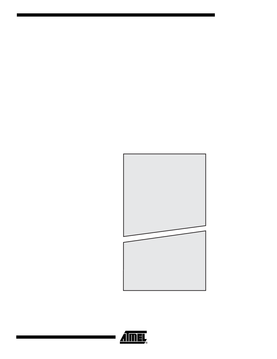
Figure 8. Program Memory Map
SRAM Data Memory
Figure 9 shows how the ATtiny2313 SRAM Memory is organized.
The lower 224 data memory locations address both the Register File, the I/O memory,
Extended I/O memory, and the internal data SRAM. The first 32 locations address the
0x0000
0x03FF
Program Memory