Ra01, Control interface, Timing specification – Rainbow Electronics RA01 User Manual
Page 9: Timing diagram
RA01
Version: 1.0 Date: 10/8/2008
Note 1: See matching circuit parameters and antenna design guide for information, and Application Notes available
from http://www.hoperf.com.
Note 2: Using other than a 10 MHz crystal is not recommended because the crystal referred timing and frequency
parameters will change accordingly.
Note 3: During this period, commands are not accepted by the chip.
Note 4: Autocalibration can be turned off.
CONTROL INTERFACE
Commands to the receiver are sent serially. Data bits on pad SDI are shifted into the device upon the rising edge of the
clock on pad SCK whenever the chip select pad nSEL is low. When the nSEL signal is high, it initializes the serial interface.
The number of bits sent is an integer multiple of 8. All commands consist of a command code, followed by a varying
number of parameter or data bits. All data are sent MSB first (e.g. bit 15 for a 16-bit command). Bits having no influence
(don’t care) are indicated with X. The Power On Reset (POR) circuit sets default values in all control registers.
The receiver will generate an interrupt request (IRQ) for the microcontroller on the following events:
• Supply voltage below the preprogrammed value is detected (LBD)
• Wake-up timer timeout (WK-UP)
• FIFO received the preprogrammed amount of bits (FFIT)
• FIFO overflow (FFOV)
FFIT and FFOV are applicable only when the FIFO is enabled. To find out why the nIRQ was issued, the status bits should
be read out.
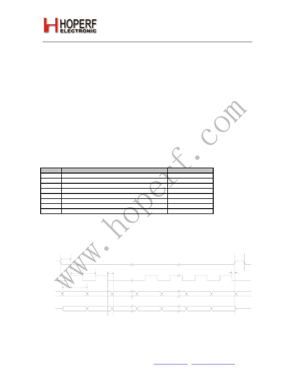
Timing Specification
Symbol
Parameter
Minimum value [ns]
t
CH
Clock high time
25
t
CL
Clock low time
25
t
SS
Select setup time (nSEL falling edge to SCK rising edge)
10
t
SH
Select hold time (SCK falling edge to nSEL rising edge)
10
t
SHI
Select high time
25
t
DS
Data setup time (SDI transition to SCK rising edge)
5
t
DH
Data hold time (SCK rising edge to SDI transition)
5
t
OD
Data delay time
10
Timing Diagram
BIT15
BIT14
BIT13
BIT8
BIT7
BIT1
BIT0
BIT15
BIT14
BIT13
BIT8
BIT7
BIT1
BIT0
tDS
tOD
tCH
tCL
tSH
tSHI
tSS
tDH
nSEL
SCK
SDI
SDO
Tel: +86-755-82973805 Fax: +86-755-82973550 E-mail: [email protected] http://www.hoperf.com
9