Ra01, Dc characteristics – Rainbow Electronics RA01 User Manual
Page 8
RA01
Version: 1.0 Date: 10/8/2008
Tel: +86-755-82973805 Fax: +86-755-82973550 E-mail: [email protected] http://www.hoperf.com
8
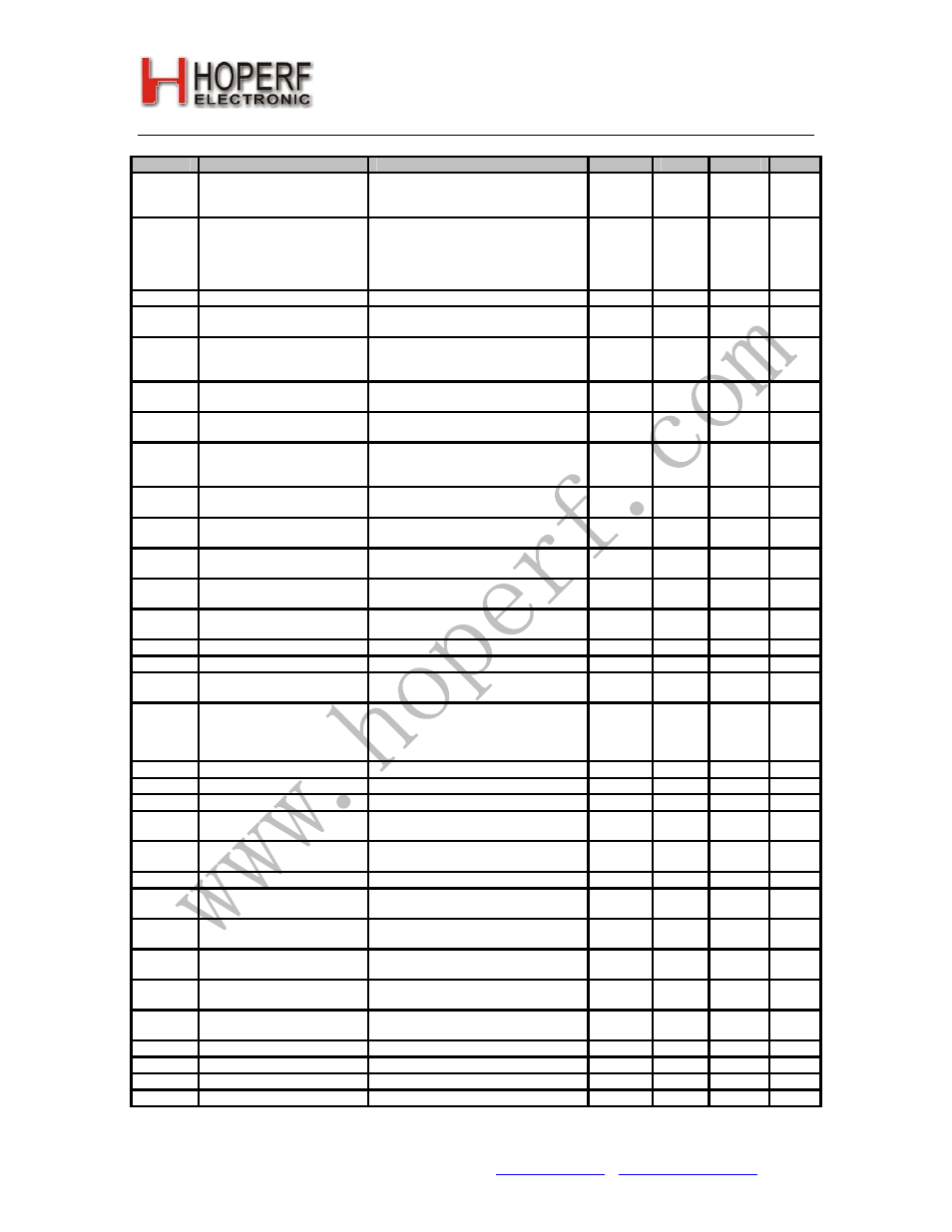
DC Characteristics
Symbol
Parameter
Conditions/Notes
Min
Typ
Max
Units
f
LO
Receiver frequency
433 MHz band, 10 kHz resolution
868 MHz band, 20 kHz resolution
915 MHz band, 20 kHz resolution
400.96
801.92
881.92
439.03
878.06
930.00
MHz
BW
Baseband fitler bandwidth
mode 1
mode 2
mode 3
mode 4
mode 5
75
125
180
235
305
85
140
200
260
340
95
155
220
295
375
kHz
BR
NRZ
OOK bit rate
with internal digital filters, NRZ data
4.8
40
kbps
BR
M
OOK bit rate
with internal digital filters,
manchester coded data
2.4
20
kbps
P
min
Receiver sensitivity
BER 3* 10
-3
, BW = 85 kHz, PN9,
BR = 9.6 kbps, Average signal
power
-110
dBm
IIP3
outh
Input IP3
out of band interferers
f-f
LO
> 5MHz
-18
dBm
CCR
Co-channel rejection
BER = 10
-2
with continuous wave
interferer in the channel
-4
dB
BR
100kHz
Blocking ratio
BER = 10
-2
with continuous wave
interferer, BW = 85 kHz,
interferer offset 100 kHz
45
dB
BR
1MHz
Blocking ratio
same as above,
interferer offset 1 MHz
50
dB
BR
10MHz
Blocking ratio
same as above,
interferer offset 10 MHz
67
dB
P
maxh
Maximum input power
LNA: high setting
min 99.99% OOK modulation
-15
dBm
P
maxa
Maximum input power
LNA: automatic or low gain setting
min 99.9% OOK modulation
0
dBm
R
in
RF input impedance real
part (differential) (Note 1)
250
Ohm
C
in
RF input capacitance
460
fF
RS
a
RSSI accuracy
+/-7
dB
RS
r
RSSI range
With automatic 32 dB LNA gain
switch
90
dB
RS
resp
DRSSI response time
Until the RSSI output goes high
after the input signal exceeds the
preprogrammed
limit, C
ARRSI
= 5nF
500
μs
f
ref
PLL reference frequency
(Note 2)
9.5
10
10.5
MHz
f
resLB
PLL frequency resolution
434 MHz Band
10
kHz
f
resHB
PLL frequency resolution
868 MHz or 915 MHz Band
20
kHz
T
settl
PLL settling time
Frequency error < 1 kHz
after 1 MHz step
30
μs
t
st1, P
PLL startup time
Initial calibration after power-up with
running crystal oscillator
500
μs
P
spur
Spurious emission
-60
dBm
C
xl
Crystal load capacitance,
see crystal selection guide
Programmable in 0.5 pF steps,
tolerance +/- 10%
8.5
16 pF
t
POR
Internal POR pulse width
(Note 3)
After V
dd
has reached 90% of final
value
50
100
ms
t
sx
Crystal oscillator startup
time
Crystal ESR < 30 Ω
5
ms
t
PBt
Wake-up timer clock period
Calibrated every 30 seconds (Note
4)
0.995
1
1.005
ms
t
wake-up
Programmable wake-up
time
1
8.4*10
6
ms
C
in, D
Digital input capacitance
2
pF
t
r, f
Digital output rise/fall time
15 pF pure capacitive load
10
ns
t
r, f ,ckout
Clock output rise/fall time
10 pF pure capacitive load
15
ns
f
ckout, slow
Slow clock frequency
Tolerance +/- 1 kHz
32
kHz