Ra01, Detailed description – Rainbow Electronics RA01 User Manual
Page 2
RA01
Version: 1.0 Date: 10/8/2008
DETAILED DESCRIPTION
General
The RA01 OOK receiver is a counterpart to the HopeRF
transmitter (e.g. RF02). It covers the unlicensed frequency
bands at 434, 868 and 915 MHz. The device facilitates
compliance with FCC and ETSI requirements.
The programmable PLL synthesizer determines the
operating frequency while preserving accuracy based on
the on-chip crystal controlled reference oscillator. The
PLL’s high resolution allows for the use of multiple
channels in any of the bands.
The receiver employs the low-IF approach with internal
demodulation, allowing the use of a minimal number of
external components in a typical application. The RA01
consists of a fully integrated multi-band PLL synthesizer,
an LNA with switchable gain, down converter mixers,
baseband filters and amplifiers, and an demodulator
followed by a data filter.
LNA
The LNA has 250 Ohm input impedance, which works well
with the recommended antennas. (See Application Notes
available from http://www.hoperf.com.)
Tel: +86-755-82973805 Fax: +86-755-82973550 E-mail: [email protected] http://www.hoperf.com
2
If the RF input of the chip is connected to 50 Ohm devices,
an external matching circuit is required to provide the
correct matching and to minimize the noise figure of the
receiver.
The LNA gain (and linearity) can be selected (0, –32 dB)
relative to the highest gain) according to RF signal
strength. This is useful in an environment with strong
interferers.
Baseband Filters
The receiver bandwidth is selectable by programming the
bandwidth (BW) of the baseband filters. This allows
setting up the receiver according to the characteristics of
the signal to be received.
An appropriate bandwidth can be selected to
accommodate various OOK deviation, data rate, and
crystal tolerance requirements. The filter structure is a 7th
order Butterworth low-pass with 40 dB suppression at
2*BW frequency. Offset cancellation is accomplished by
using a high-pass filter with a 90 kHz cut-off frequency.
Filter bandwidth is measured between the 6dB attenuation
points.
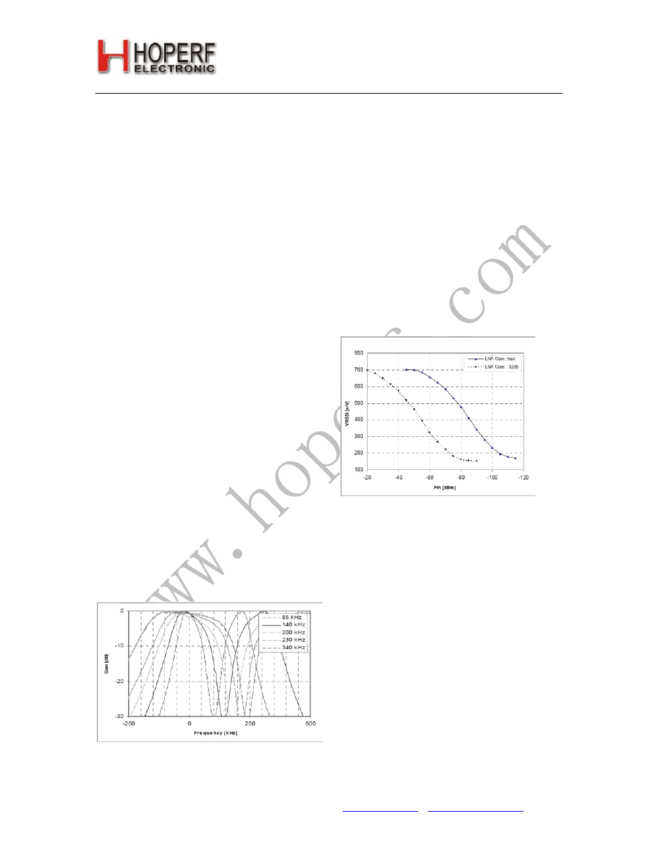
Typical Baseband Filter Characteristics
Data Filtering and Clock Recovery
The output data filtering can be completed by an
external capacitor to the final application.
Analog operation: The filter is an RC type low-pass
filter and a Schmitt-trigger (St). The resistor (10k) and
the St is integrated on the chip. An (external) capacitor
can be chosen according to the
actual bit-rate.
Data Validity Blocks / Demodulator
RSSI
A digital RSSI output is provided to monitor the input
signal level. It goes to an comparator, if the received
signal strength exceeds a given preprogrammed level
an internal -32dB attenuator is activated in the LNA.
The RSSI settling time depends on the filter capacitor
used.
Typical Analog RSSI Voltage vs. RF Input Power
Crystal Oscillator and
Microcontroller Clock Output
The chip has a single-pin crystal oscillator circuit,
which provides a 10 MHz reference signal for the PLL.
To reduce external parts and simplify design, the
crystal load capacitor is internal and programmable.
Guidelines for selecting the appropriate crystal can
be found later in this datasheet. The receiver can
supply the clock signal for the microcontroller, so
accurate timing is possible without the need for a
second crystal. In normal operation it is divided from
the reference 10 MHz. During sleep mode a low
frequency (typical 32 kHz) output clock signal can be
switched on.
When the microcontroller turns the crystal oscillator off
by clearing the appropriate bit using the
Configuration
Setting Command,
the chip provides a programmable
number (default is 128) of further clock pulses (“clock
tail”) for the microcontroller to let it go to idle or sleep
mode.