Pin description – Rainbow Electronics MAX7033 User Manual
Page 8
MAX7033
315MHz/433MHz ASK Superheterodyne
Receiver with AGC Lock
8
_______________________________________________________________________________________
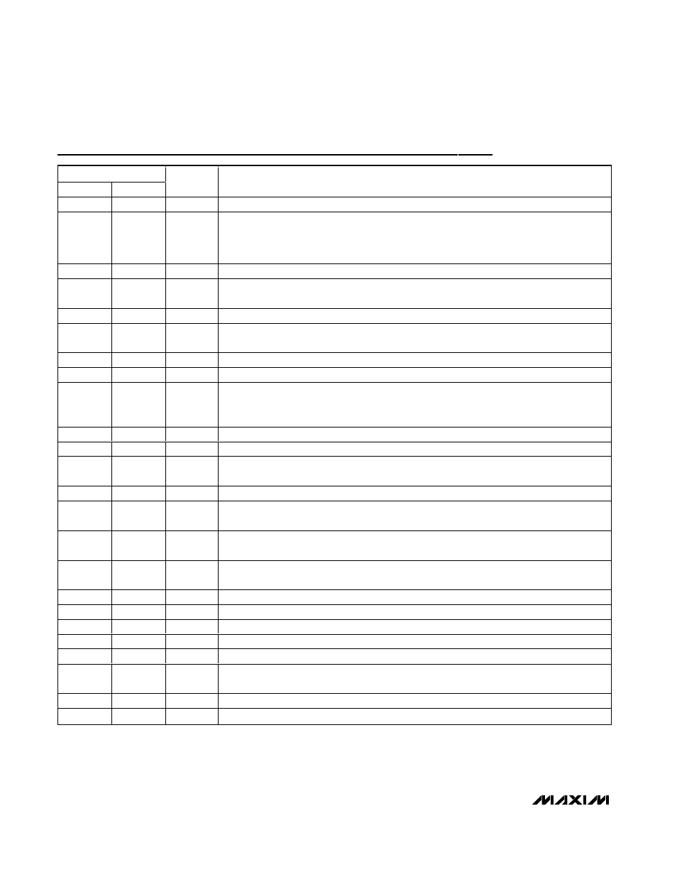
Pin Description
PIN
TSSOP
THIN QFN
NAME
FUNCTION
1
29
XTAL1
Crystal Input 1 (See the Phase-Locked Loop section)
2, 7
4, 30
AV
DD
Positive Analog Supply Voltage. For +5V operation, AV
DD
is connected to an on-chip +3.2V
low-dropout regulator. Both AV
DD
pins must be externally connected to each other. Bypass
each pin to AGND with a 0.01µF capacitor as close to the pin as possible (see the Typical
Application Circuit).
3
31
LNAIN
Low-Noise Amplifier Input (See the Low-Noise Amplifier section)
4
32
LNASRC
Low-Noise Amplifier Source for External Inductive Degeneration. Connect inductor to ground
to set the LNA input impedance (see the Low-Noise Amplifier section).
5, 10
2, 7
AGND
Analog Ground
6
3
LNAOUT
Low-Noise Amplifier Output. Connect to mixer input through an LC tank filter (see the Low-
Noise Amplifier section).
8
5
MIXIN1
1st Differential Mixer Input. Connect to LC tank filter from LNAOUT.
9
6
MIXIN2
2nd Differential Mixer Input. Connect through a 100pF capacitor to AV
DD
side of the LC tank.
11
8
IRSEL
Image-Rejection Select. Set V
IRSEL
= 0V to center image rejection at 315MHz. Leave IRSEL
unconnected to center image rejection at 375MHz. Set V
IRSEL
= V
DD5
to center image
rejection at 433MHz.
12
9
MIXOUT
330
Ω Mixer Output. Connect to the input of the 10.7MHz bandpass filter.
13
10
DGND
Digital Ground
14
11
DV
DD
Positive Digital Supply Voltage. Connect to AV
DD
. Bypass to DGND with a 0.01µF capacitor
as close to the pin as possible.
15
12
AC
Automatic Gain Control. See Figure 1. Internally pulled down to AGND with a 100k
Ω resistor.
16
14
XTALSEL
Crystal Divider Ratio Select. Drive XTALSEL low to select divider ratio of 64, or drive
XTALSEL high to select divider ratio of 32.
17
15
IFIN1
1st Differential Intermediate-Frequency Limiter Amplifier Input. Bypass to AGND with a
1500pF capacitor as close to the pin as possible.
18
16
IFIN2
2nd Differential Intermediate-Frequency Limiter Amplifier Input. Connect to the output of a
10.7MHz bandpass filter.
19
17
DFO
Data Filter Output
20
18
DSN
Negative Data Slicer Input
21
19
OPP
Noninverting Op-Amp Input for the Sallen-Key Data Filter
22
20
DFFB
Data-Filter Feedback Node. Input for the feedback of the Sallen-Key data filter.
23
22
DSP
Positive Data Slicer Input
24
23
V
DD5
+5V Supply Voltage. For +5V operation, V
DD5
is the input to an on-chip voltage regulator
whose +3.2V output drives AV
DD
.
25
24
DATAOUT Digital Baseband Data Output
26
26
PDOUT
Peak-Detector Output