Applications information – Rainbow Electronics MAX7033 User Manual
Page 11
MAX7033
315MHz/433MHz ASK Superheterodyne
Receiver with AGC Lock
______________________________________________________________________________________
11
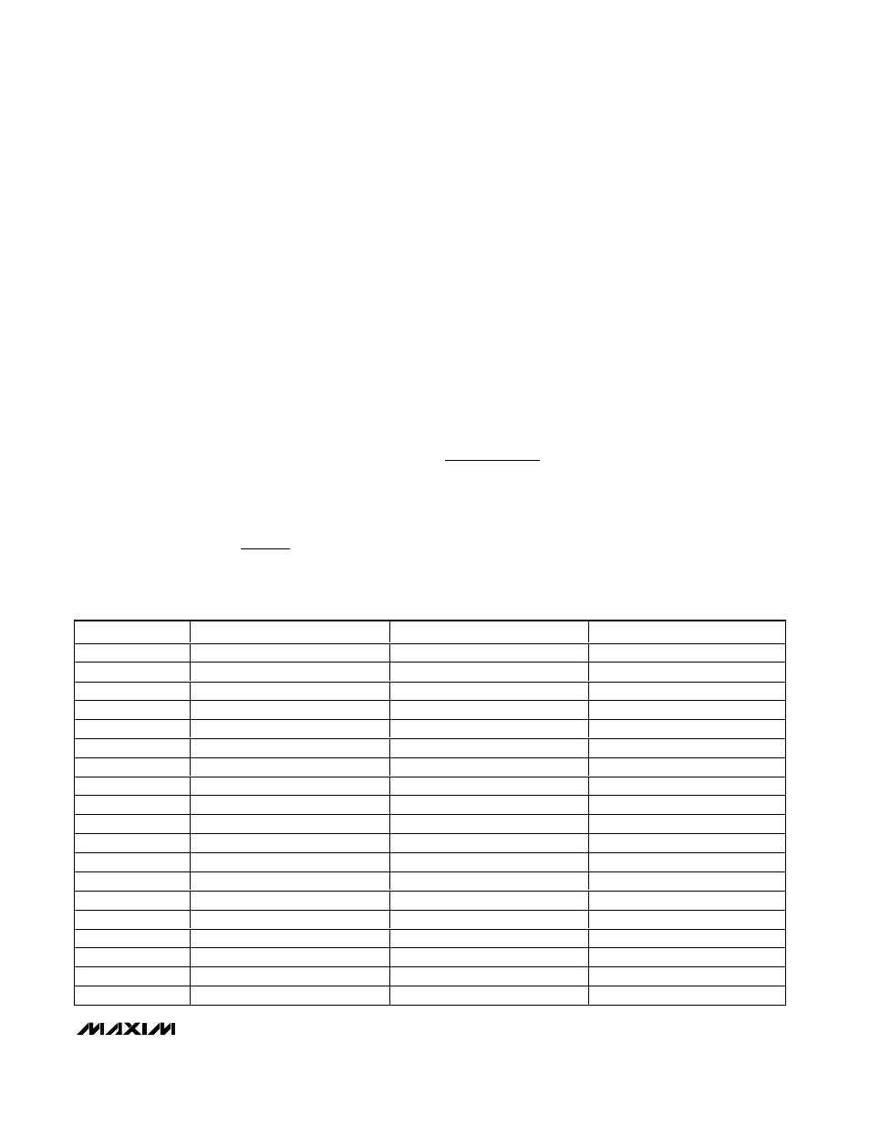
COMPONENT
VALUE FOR f
RF
= 433MHz
VALUE FOR f
RF
= 315MHz
DESCRIPTION
L1
56nH
120nH
TOKO LL1608-FH
L2
15nH
15nH
Murata LQP11A
L3
15nH
27nH
Murata LQP11A
C1
100pF
100pF
5%
C2
2pF
4pF
± 0.1pF
C3
100pF
100pF
5%
C4
100pF
100pF
5%
C5
1500pF
1500pF
10%
C6
220pF
220pF
5%
C7
470pF
470pF
5%
C8
0.47µF
0.47µF
20%
C9
220pF
220pF
10%
C10
0.01µF
0.01µF
20%
C11
0.01µF
0.01µF
20%
C12
15pF
15pF
Depends on XTAL
C13
15pF
15pF
Depends on XTAL
R1
5.1k
Ω
5.1k
Ω
5%
X1
6.5984MHz
4.7547MHz
—
X2
10.7MHz ceramic filter
10.7MHz ceramic filter
Murata SFECV10.7 series
injection is required due to the on-chip image-rejection
architecture. The IF output is driven by a source follow-
er biased to create a driving-point impedance of 330
Ω;
this provides a good match to the off-chip 330
Ω ceram-
ic IF filter.
The IRSEL pin is a logic input that selects one of the
three possible image-rejection frequencies. When V
IRSEL
= 0V, the image rejection is tuned to 315MHz. V
IRSEL
=
V
DD5
/ 2 tunes the image rejection to 375MHz, and
V
IRSEL
= V
DD5
tunes the image rejection to 433MHz. The
IRSEL pin is internally set to V
DD5
/ 2 (image rejection at
375MHz) when it is left unconnected, thereby eliminating
the need for an external V
DD5
/ 2 voltage.
Phase-Locked Loop
The PLL block contains a phase detector, charge
pump, integrated loop filter, VCO, asynchronous 64x
clock divider, and crystal oscillator driver. Besides the
crystal, this PLL does not require any external compo-
nents. The VCO generates a low-side LO. The relation-
ship between the RF, IF, and reference frequencies is
given by:
where:
M = 1 (V
XTALSEL
= V
DD5
) or 2 (V
XTALSEL
= 0V)
To allow the smallest possible IF bandwidth (for best sen-
sitivity), minimize the tolerance of the reference crystal.
Intermediate Frequency and RSSI
The IF section presents a differential 330
Ω load to pro-
vide matching for the off-chip ceramic filter. The six
internal AC-coupled limiting amplifiers produce an
overall gain of approximately 65dB, with a bandpass-fil-
ter-type response centered near the 10.7MHz IF fre-
quency with a 3dB bandwidth of approximately 10MHz.
The RSSI circuit demodulates the IF by producing a DC
output proportional to the log of the IF signal level, with
a slope of approximately 14.2mV/dB (see the Typical
Operating Characteristics).
Applications Information
Crystal Oscillator
The crystal oscillator in the MAX7033 is designed to
present a capacitance of approximately 3pF between
the XTAL1 and XTAL2. If a crystal designed to oscillate
with a different load capacitance is used, the crystal is
pulled away from its stated operating frequency, intro-
ducing an error in the reference frequency. Crystals
f
f
f
M
REF
RF
IF
=
×
-
32
Table 1. Component Values for Typical Application Circuit