Functional diagram, Detailed description, Voltage regulator – Rainbow Electronics MAX7034 User Manual
Page 8: Low-noise amplifier
MAX7034
315MHz/434MHz ASK Superheterodyne
Receiver
8
_______________________________________________________________________________________
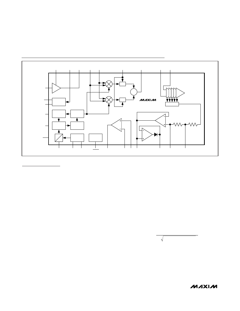
Functional Diagram
LNAOUT
MIXIN1 MIXIN2
0˚
90˚
IFIN1
MIXOUT
IFIN2
RSSI
R
DF2
100k
Ω
R
DF1
100k
Ω
DIVIDE
BY 64
VCO
LOOP
FILTER
PHASE
DETECTOR
CRYSTAL
DRIVER
POWER-
DOWN
IF LIMITING
AMPS
14
LNASRC
DATA
SLICER
DATA
FILTER
Q
∑
I
IMAGE
REJECTION
3.4V REG
24
2, 7
IRSEL
13
5, 10
AV
DD
V
DD5
DV
DD
DGND
AGND
LNAIN
3
XTALSEL
16
XTAL1
1
XTAL2
28
SHDN
27
DATAOUT
25
DSN
20
DSP
23
DFO
19
PDOUT
26
OPP
21
DFFB
22
4
15
6
8
9
11
12
17
18
EN_REG
ч2
ч1
MAX7034
LNA
Detailed Description
The MAX7034 CMOS superheterodyne receiver and a
few external components provide the complete receive
chain from the antenna to the digital output data.
Depending on signal power and component selection,
data rates can be as high as 33kbps Manchester
(66kbps NRZ).
The MAX7034 is designed to receive binary ASK data
modulated in the 300MHz to 450MHz frequency range.
ASK modulation uses a difference in amplitude of the
carrier to represent logic 0 and logic 1 data.
Voltage Regulator
The MAX7034 is designed to work with a nominal +5.0V
supply voltage. The MAX7034 integrates an internal volt-
age regulator that provides +3.4V to some of the internal
circuits in the device; this voltage is connected to the
AVDD and DVDD pins. The device can be operated from
+3.0V to +3.6V by pulling the EN_REG pin low (which dis-
ables the internal voltage regulator) and connecting the
supply voltage to the AVDD and DVDD pins. If the
MAX7034 is powered from +3.0 to +3.6V, the perfor-
mance is limited to the -40°C to +105°C range.
Low-Noise Amplifier
The LNA is an nMOS cascode amplifier with off-chip
inductive degeneration. The gain and noise figures are
dependent on both the antenna matching network at
the LNA input and the LC tank network between the
LNA output and the mixer inputs.
The off-chip inductive degeneration is achieved by
connecting an inductor from LNASRC to AGND. This
inductor sets the real part of the input impedance at
LNAIN, allowing for a more flexible input impedance
match, such as a typical printed-circuit board (PCB)
trace antenna. A nominal value for this inductor with a
50Ω input impedance is 15nH, but is affected by the
PCB trace.
The LC tank filter connected to LNAOUT comprises L1
and C9 (see the
Typical Application Circuit
). Select L1
and C9 to resonate at the desired RF input frequency.
The resonant frequency is given by:
where:
L
TOTAL
= L1 + L
PARASITICS
.
C
TOTAL
= C9 + C
PARASITICS
.
L
PARASITICS
and C
PARASITICS
include inductance and
capacitance of the PCB traces, package pins, mixer
input impedance, etc. These parasitics at high frequen-
cies cannot be ignored, and can have a dramatic effect
f
L
C
RF
TOTAL
TOTAL
=
×
1
2
π