Pin description – Rainbow Electronics MAX7034 User Manual
Page 7
MAX7034
315MHz/434MHz ASK Superheterodyne
Receiver
_______________________________________________________________________________________
7
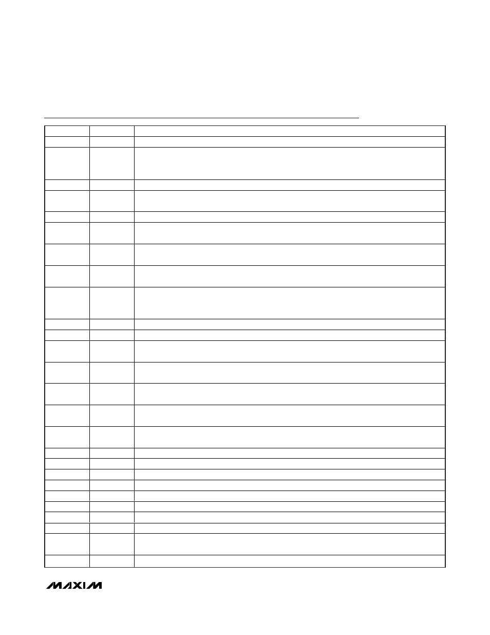
Pin Description
PIN
NAME
FUNCTION
1
XTAL1
Crystal Input 1
2, 7
AV
DD
P osi ti ve Anal og S up p l y V ol tag e. AV
DD
i s connected to an on- chi p + 3.4V l ow - d r op out r eg ul ator . Both
AV
DD
p i ns m ust b e exter nal l y connected to each other . Byp ass p i n 2 to AG N D w i th a 0.1µF cap aci tor as
cl ose as p ossi b l e to the p i n ( see the Typ i cal Ap p l i cati on C i r cui t) . Byp ass p i n 7 w i th a 0.01µF cap aci tor .
3
LNAIN
Low-Noise Amplifier Input. See the Low-Noise Amplifier section.
4
LNASRC
Low-Noise Amplifier Source for external Inductive Degeneration. Connect inductor to ground to set
LNA input impedance. See the Low-Noise Amplifier section.
5, 10
AGND
Analog Ground
6
LNAOUT
Low-Noise Amplifier Output. Connect to mixer input through an LC tank filter. See the Low-Noise
Amplifier section.
8
MIXIN1
1st Differential Mixer Input. Connect to LC tank filter from LNAOUT through a 100pF capacitor. See
the Typical Application Circuit.
9
MIXIN2
2nd Differential Mixer Input. Connect to AV
DD
side of the LC tank filter through a 100pF capacitor.
See the Typical Application Circuit.
11
IRSEL
Image-Rejection Select. Set V
IRSEL
= 0V to center image rejection at 315MHz. Leave IRSEL
unconnected to center image rejection at 375MHz. Set V
IRSEL
= DV
DD
to center image rejection at
434MHz. See the Mixer section.
12
MIXOUT
330
Ω Mixer Output. Connect to the input of the 10.7MHz bandpass filter.
13
DGND
Digital Ground
14
DV
DD
Positive Digital Supply Voltage. Connect to AV
DD
. Bypass to DGND with a 0.01µF capacitor as close
as possible to the pin.
15
EN_REG
Regulator Enable. Connect to V
DD5
to enable internal regulator. Pull this pin low to allow device
operation between +3.0V and +3.6V. See the Voltage Regulator section.
16
XTALSEL
Crystal Divider Ratio Select. Drive XTALSEL low to select divider ratio of 64, or drive XTALSEL high to
select divider ratio of 32.
17
IFIN1
1st Differential Intermediate-Frequency Limiter Amplifier Input. Connect to the output of a 10.7MHz
bandpass filter.
18
IFIN2
2nd Differential Intermediate-Frequency Limiter Amplifier Input. Bypass to AGND with a 1500pF
capacitor as close as possible to the pin.
19
DFO
Data Filter Output
20
DSN
Negative Data Slicer Input
21
OPP
Noninverting Op-Amp Input for the Sallen-Key Data Filter
22
DFFB
Data Filter Feedback Node. Input for the feedback of the Sallen-Key data filter.
23
DSP
Positive Data Slicer Input
24
V
DD5
+5.0V Supply Voltage
25
DATAOUT
Digital Baseband Data Output
26
PDOUT
Peak-Detector Output
27
SHDN
Power-Down Select Input. Drive high to power up the IC. Internally pulled down to AGND with a
100k
Ω resistor.
28
XTAL2
C r ystal Inp ut 2. C an al so b e d r i ven w i th an exter nal r efer ence osci l l ator . S ee the C r ystal O sci l l ator secti on.