NEC uPD78P078 User Manual
Page 589
589
CHAPTER 28 INSTRUCTION SET
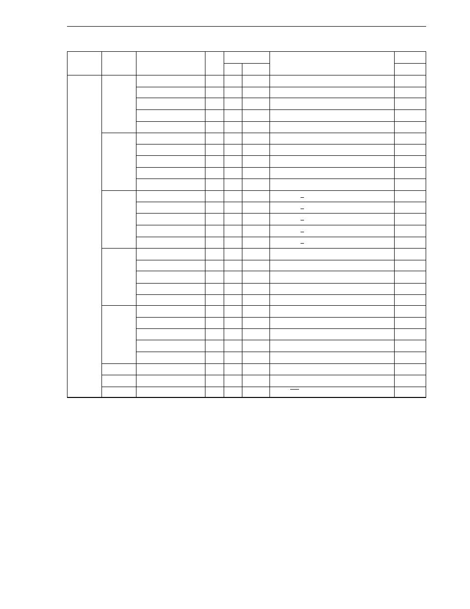
Instruction
Mnemonic
Operands
Byte
Clock
Operation
Flag
Group
Note 1
Note 2
Z AC CY
Bit mani-
AND1
CY, saddr.bit
3
6
7
CY
←
CY /\ (saddr.bit)
x
pulation
CY, sfr.bit
3
—
7
CY
←
CY /\ sfr.bit
x
CY, A.bit
2
4
—
CY
←
CY /\ A.bit
x
CY, PSW.bit
3
—
7
CY
←
CY /\ PSW.bit
x
CY, [HL].bit
2
6
7 + n
CY
←
CY /\ (HL).bit
x
OR1
CY, saddr.bit
3
6
7
CY
←
CY \/ (saddr.bit)
x
CY, sfr.bit
3
—
7
CY
←
CY \/ sfr.bit
x
CY, A.bit
2
4
—
CY
←
CY \/ A.bit
x
CY, PSW.bit
3
—
7
CY
←
CY \/ PSW.bit
x
CY, [HL].bit
2
6
7 + n
CY
←
CY \/ (HL).bit
x
XOR1
CY, saddr.bit
3
6
7
CY
←
CY \/ (saddr.bit)
x
CY, sfr.bit
3
—
7
CY
←
CY \/ sfr.bit
x
CY, A.bit
2
4
—
CY
←
CY \/ A.bit
x
CY, PSW. bit
3
—
7
CY
←
CY \/ PSW.bit
x
CY, [HL].bit
2
6
7 + n
CY
←
CY \/ (HL).bit
x
SET1
saddr.bit
2
4
6
(saddr.bit)
←
1
sfr.bit
3
—
8
sfr.bit
←
1
A.bit
2
4
—
A.bit
←
1
PSW.bit
2
—
6
PSW.bit
←
1
x
x
x
[HL].bit
2
6
8+n+m
(HL).bit
←
1
CLR1
saddr.bit
2
4
6
(saddr.bit)
←
0
sfr.bit
3
—
8
sfr.bit
←
0
A.bit
2
4
—
A.bit
←
0
PSW.bit
2
—
6
PSW.bit
←
0
x
x
x
[HL].bit
2
6
8+n+m
(HL).bit
←
0
SET1
CY
1
2
—
CY
←
1
1
CLR1
CY
1
2
—
CY
←
0
0
NOT1
CY
1
2
—
CY
←
CY
x
Notes 1. For instructions that access the internal high-speed RAM area or perform no data access
2. For instructions that access an area other than the internal high-speed RAM area
Remarks 1. One clock in the “Clock” columns is equal to one cycle of the CPU clock (f
CPU
) selected by the processor
clock control register (PCC).
2. The values in the “Clock” column assumes that the internal ROM area contains programs.
3. n indicates wait cycles to be inserted when an external expansion memory area is read from.
4. m indicates wait cycles to be inserted when an external expansion memory area is written to.