NEC uPD78P078 User Manual
Page 152

152
CHAPTER 6 PORT FUNCTIONS
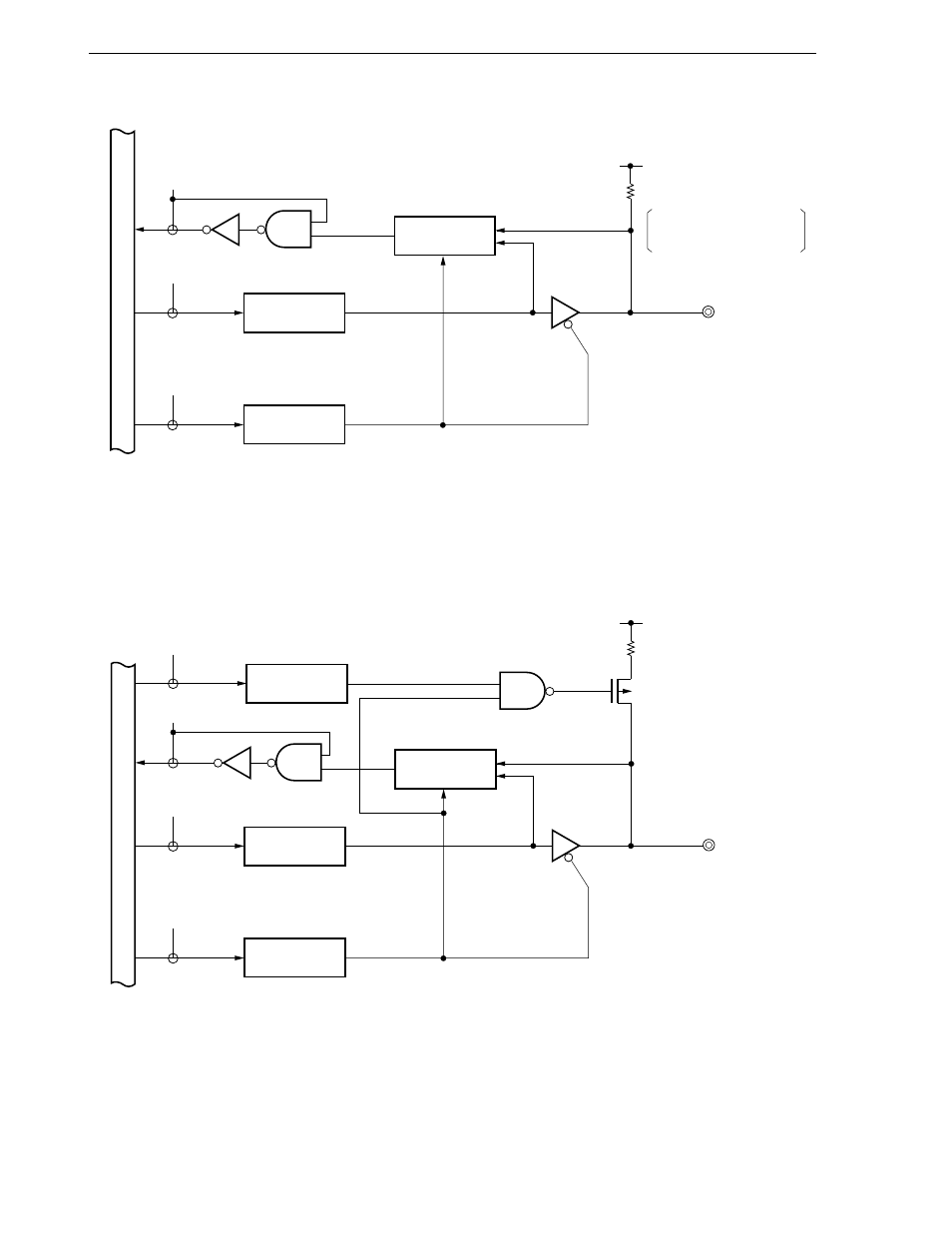
Figure 6-18. Block Diagram of P90 to P93
PM
: Port mode register
RD
: Port 9 read signal
WR : Port 9 write signal
Figure 6-19. Block Diagram of P94 to P96
PUO : Pull-up resistor option register
PM
: Port mode register
RD
: Port 9 read signal
WR : Port 9 write signal
Mask Option Resistor
WR
PM
WR
PORT
RD
V
DD
Selector
Output Latch
(P90 to P93)
PM90 to PM93
Internal bus
P90 to P93
Mask ROM versions only.
PD78P078 and 78P078Y
have no pull-up resistor.
µ
P-ch
WR
PM
WR
PORT
RD
WR
PUO
V
DD
Selector
PUO9
Output Latch
(P94 to P96)
PM94 to PM96
Internal bus
P94 to P96
