149
CHAPTER 6 PORT FUNCTIONS
P-ch
WR
PM
WR
PORT
RD
WR
PUO
V
DD
Selector
PUO7
Output Latch
(P71, P72)
PM71, PM72
Internal bus
Dual Function
P71/SO2/TxD,
P72/SCK2/ASCK
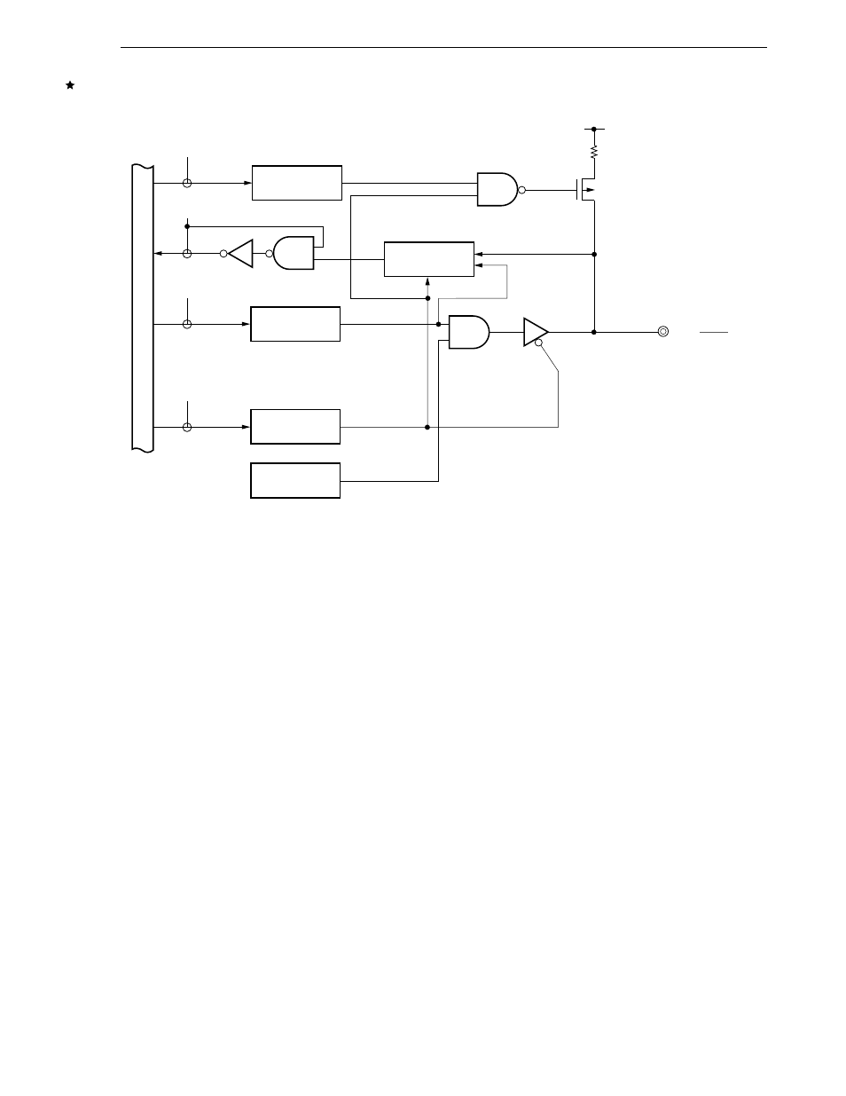
Figure 6-16. Block Diagram of P71 and P72
PUO : Pull-up resistor option register
PM
: Port mode register
RD
: Port 7 read signal
WR : Port 7 write signal