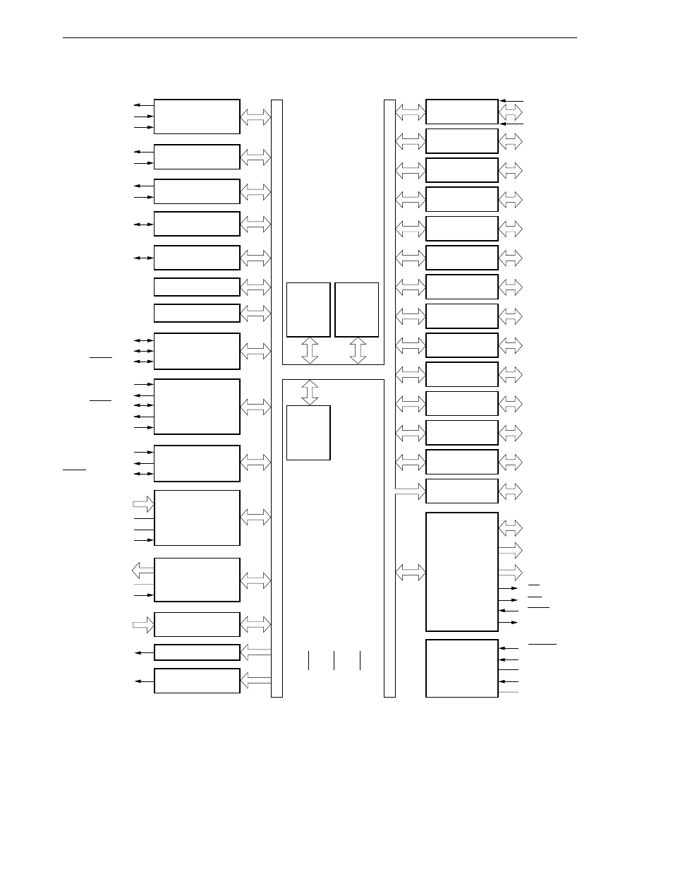
7 block diagram – NEC uPD78P078 User Manual
Page 44

44
CHAPTER 1 OUTLINE (
µ
PD78078 SUBSERIES)
1.7 Block Diagram
Remarks 1. The internal ROM and RAM capacities depend on the product.
2. Pin connection in parentheses is for the
µ
PD78P078.
TO0/P30
TI00/INTP0/P00
TI01/INTP1/P01
Interrupt
Control
Serial
Interface 1
A/D Converter
Serial
Interface 0
Watchdog Timer
8-bit TIMER/
Event Counter 1
16-bit TIMER/
Event Counter
Port 0
External
Access
P01 to P06
8-bit TIMER/
Event Counter 2
Port 1
P10 to P17
Port 2
P20 to P27
Port 3
P30 to P37
Port 4
P40 to P47
Port 5
P50 to P57
Port 6
P60 to P67
Port 7
P70 to P72
Port 8
P80 to P87
Port 9
P90 to P96
Port 10
P100 to P103
Port 12
P120 to P127
Port 13
P130, P131
Real-Time
Output Port
RTP0/P120 to
RTP7/P127
System
Control
AD0/P40 to
AD7/P47
A0/P80 to
A7/P87
A8/P50 to
A15/P57
RD/P64
WR/P65
WAIT/P66
ASTB/P67
RESET
X1
X2
XT1/P07
XT2
V
DD
V
SS
IC
(V
PP
)
RAM
78K/0
CPU Core
ROM
8-bit TIMER/
Event Counter 5
8-bit TIMER/
Event Counter 6
Watch Timer
Serial
Interface 2
D/A Converter
Buzzer Output
Clock Output
Control
TO1/P31
TI1/P33
TO2/P32
TI2/P34
TI5/TO5/P100
TI6/TO6/P101
SI0/SB0/P25
SO0/SB1/P26
SCK0/P27
SI1/P20
SO1/P21
SCK1/P22
STB/P23
BUSY/P24
SI2/RxD/P70
SO2/TxD/P71
SCK2/ASCK/P72
AV
DD
AV
SS
AV
REF0
ANI0/P10 to
ANI7/P17
AV
SS
AV
REF1
ANO0/P130,
ANO1/P131
INTP0/P00 to
INTP6/P06
BUZ/P36
PCL/P35
P00
P07
