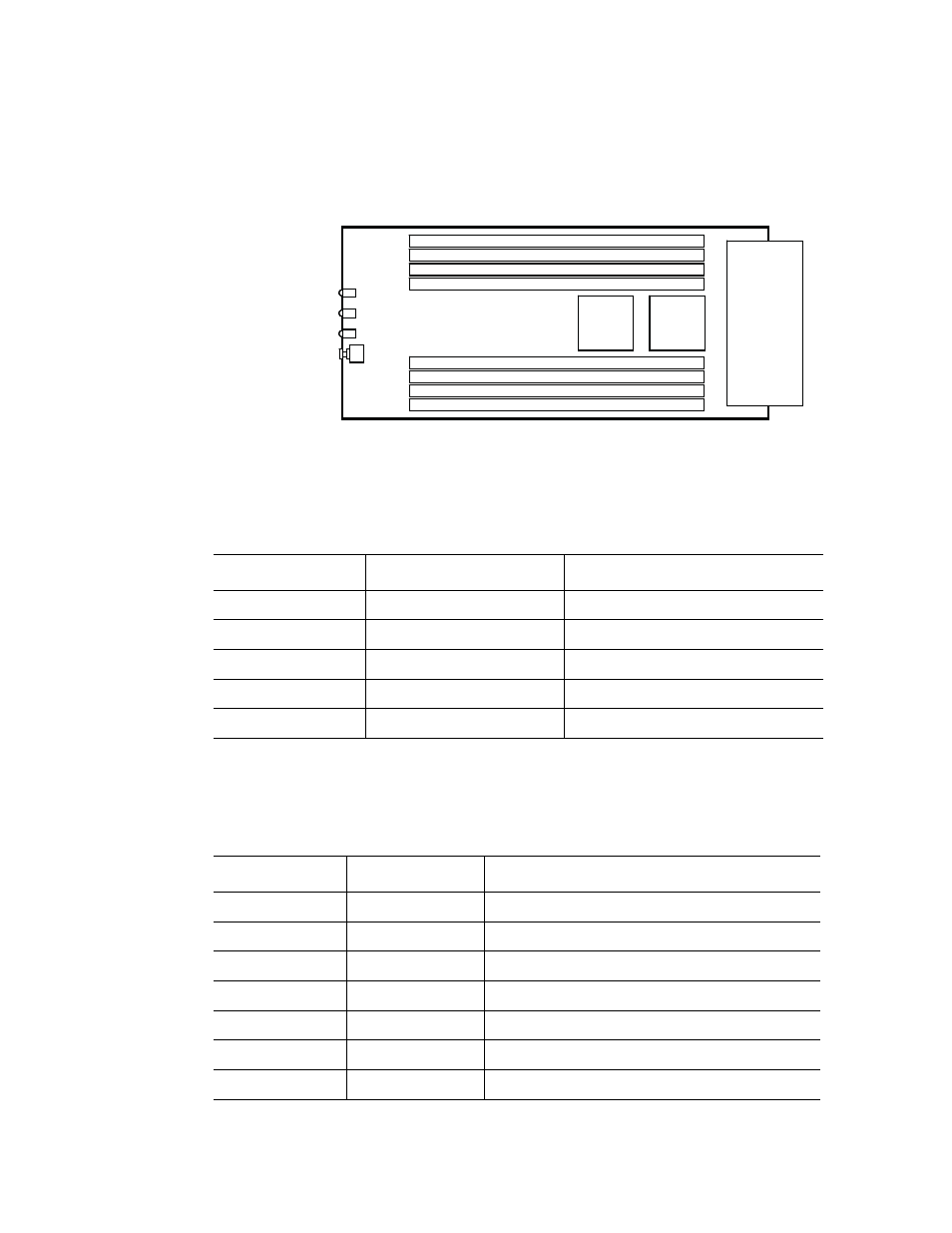
Memory box card, Figure 15. memory box card layout – Intel SR9000MK4U User Manual
Page 46

24
Intel
®
Server System SR9000MK4U Product Guide
Memory Box Card
Figure 15. Memory Box Card Layout
Table 12. Memory Box Card Components
Board Location
Component
Description
P1/P2
MC0/2
Memory Controller
P3
Mirror LED
See
.
P4
Attention LED
See
.
P5
Power LED
See
.
P6
Hot Swap Button
Table 13. Memory Box Card Connectors
Board Location
Connector
Description
C1
JD0B1
240-pin DDR2 DIMM socket (MC0 channel A)
C2
JD0B0
240-pin DDR2 DIMM socket (MC0 channel A)
C3
JD0A1
240-pin DDR2 DIMM socket (MC0 channel B)
C4
JD0A0
240-pin DDR2 DIMM socket (MC0 channel B)
C5
JD2B1
240-pin DDR2 DIMM socket (MC1 channel A)
C6
JD2B0
240-pin DDR2 DIMM socket (MC1 channel A)
C7
JD2A1
240-pin DDR2 DIMM socket (MC1 channel B)
AF001096
JD0A0
JD0A1
JD0B0
JD0B1
JD2B1
JD2B0
JD2A1
JD2A0
MC2
MC0
VHDM
Attention LED
Mirror LED
Power LED
Hot Swap SW
P1
P2
P3
P4
P5
P6
c1
c2
c3
c4
c8
c7
c6
c5
c9
