Figure3.4 lvd driver, Lvd driver, Lvd driver scsi signals—b_sd[15:0 – Avago Technologies LSI53C180 User Manual
Page 43: Lvd receiver scsi signals—b_sd[15:0
Electrical Characteristics
3-9
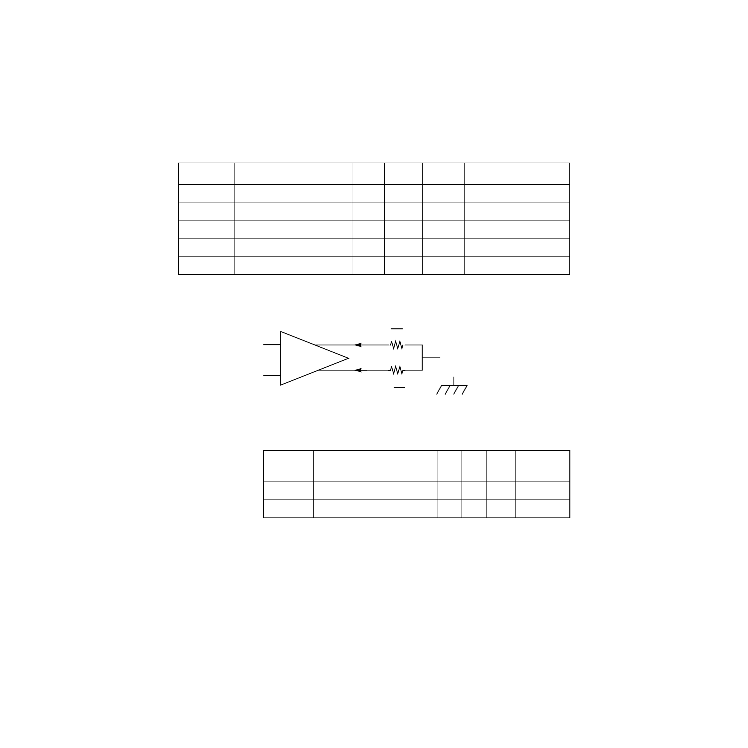
Figure 3.4
LVD Driver
Table 3.7
LVD Driver SCSI Signals—B_SD[15:0]
±
, B_SDP[1:0]
±
, B_SCD
±
, B_SIO
±
,
B_SMSG
±
, B_SREQ
±
, B_SACK
±
, B_SBSY
±
, B_SATN
±
, B_SSEL
±
,
B_SRST
±
1
Symbol
Parameter
Min
Max
Units
Test Conditions
I
O
+
Source (+) current
9.6
14.4
mA
Asserted state
I
O
−
Sink (
−
) current
−
9.6
−
14.4
mA
Asserted state
I
O
+
Source (+) current
−
6.4
−
9.6
mA
Negated state
I
O
−
Sink (
−
) current
6.4
9.6
mA
Negated state
I
OZ
3-state leakage
−
20
20
µ
A
V
PIN
= 0 V, 3.47 V
1. V
CM
= 0.7
−
1.8 V, R
L
= 0
−
110
Ω,
R
bias
= 10 k
Ω.
Table 3.8
LVD Receiver SCSI Signals—B_SD[15:0]
±
,
B_SDP[1:0]
±
, B_SCD
±
, B_SIO
±
, B_SMSG
±
, B_SREQ
±
,
B_SACK
±
, B_SBSY
±
, B_SATN
±
, B_SSEL
±
, B_SRST
±
1
1. V
CM
= 0.7
−
1.8 V.
Symbol
Parameter
Min
Max
Units
Test
Conditions
V
I
LVD receiver voltage asserting
60
–
mV
–
V
I
LVD receiver voltage negating
–
−
60
mV
–
+
−
R
L
2
V
CM
+
I
O
+
R
L
2
I
O
−
−
- MGA-725M4 (4 pages)
- MGA-71543 (4 pages)
- MGA-71543 (3 pages)
- MGA-82563 (6 pages)
- 3ware SAS 9750-8i (48 pages)
- 3ware 9690SA-8I (Channel) (138 pages)
- 3ware 9690SA-8I (Channel) (380 pages)
- 3ware SAS 9750-8i (29 pages)
- 3ware 9550SXU-8LP (Channel) (149 pages)
- 3ware 9550SXU-8LP (Channel) (40 pages)
- 3ware 9650SE-8LPML (Channel) (45 pages)
- 3ware 9690SA-8I (Channel) (27 pages)
- 3ware 9690SA-8I (Channel) (361 pages)
- 6160 SAS Switch (2 pages)
- MegaRAID SAS 9266-8i (12 pages)
- MegaRAID SAS 9380-8e (43 pages)
- Cache Protection for RAID Controller Cards (139 pages)
- Cache Protection for RAID Controller Cards (13 pages)
- MegaRAID SAS 9271-8iCC (13 pages)
- MegaRAID SAS 9361-8i (13 pages)
- MegaRAID SAS 9266-8i (20 pages)
- MegaRAID SAS 9271-8iCC (26 pages)
- MegaRAID SafeStore Software (502 pages)
- MegaRAID SAS 9285-8ecv (80 pages)
- MegaRAID SAS 9285-8ecv (92 pages)
- MegaRAID SAS 0260CV-4i (64 pages)
- MegaRAID SAS 0260CV-4i (49 pages)
- MegaRAID SAS 9271-8i (8 pages)
- MegaRAID SAS 0260CV-4i (72 pages)
- MegaRAID SAS 9361-8i (7 pages)
- MegaRAID SAS 9341-8i (8 pages)
- MegaRAID SAS 9380-4i4e (7 pages)
- MegaRAID SAS 9380-8e (7 pages)
- MegaRAID SAS 0260CV-4i (28 pages)
- MegaRAID SAS 9240-8i (4 pages)
- MegaRAID SAS 9260-16i (12 pages)
- MegaRAID SAS 9280-24i4e (14 pages)
- MegaRAID SAS 9280-24i4e (16 pages)
- MegaRAID SAS 9260-8i (4 pages)
- MegaRAID SafeStore Software (8 pages)
- MegaRAID SAS 9280-8e (22 pages)
- MegaRAID SAS 9261-8i (4 pages)
- MegaRAID SAS 9285-8e (12 pages)
- MegaRAID SAS 9280-16i4e (12 pages)
- MegaRAID SAS 9280-4i4e (4 pages)