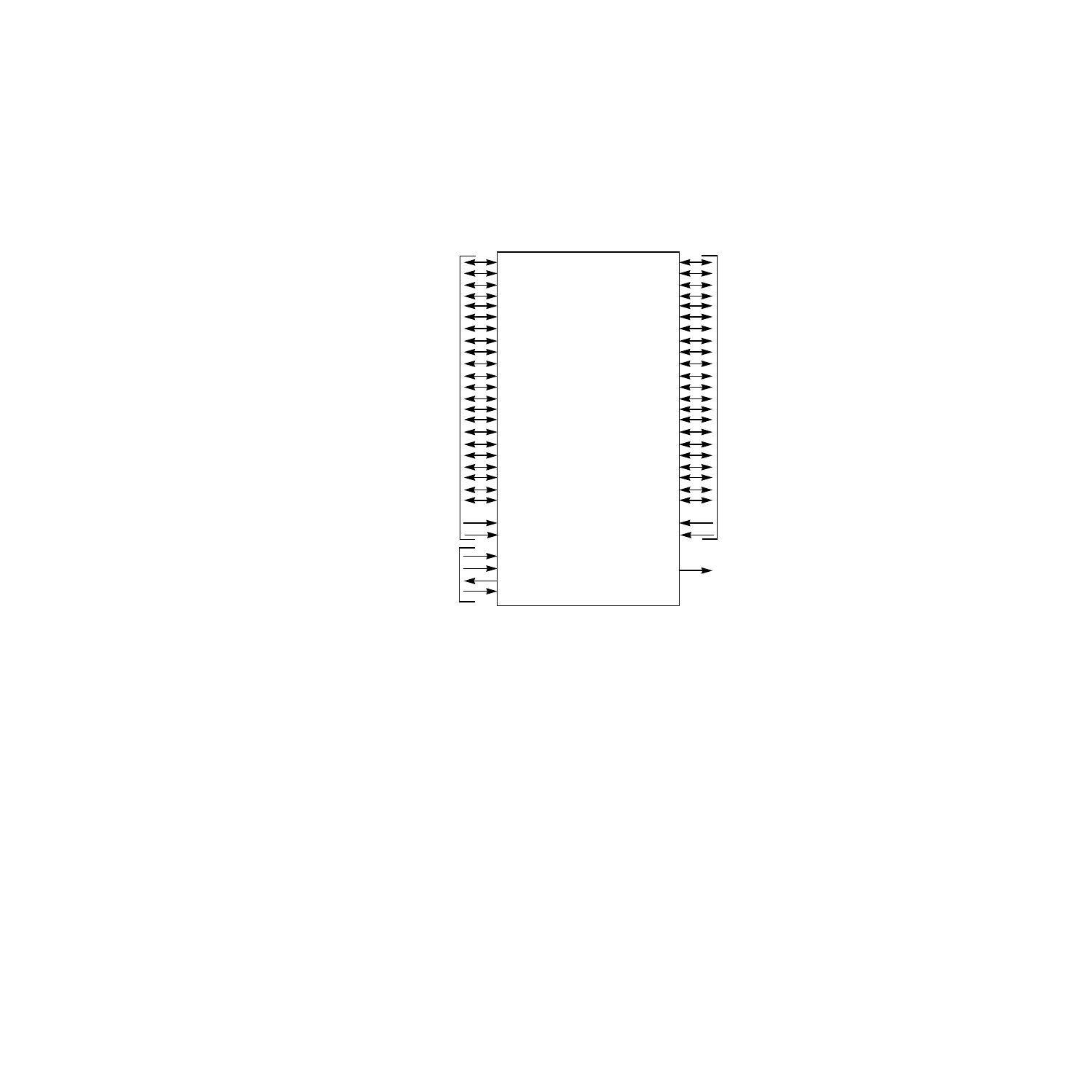
Figure2.2 lsi53c180 signal grouping, Lsi53c180 signal grouping – Avago Technologies LSI53C180 User Manual
Page 24

2-6
Functional Descriptions
Section 3.2.4, “SCSI Interface Timing.” Figure 2.2
shows the LSI53C180
signal grouping. A description of the signal groups follows.
Figure 2.2
LSI53C180 Signal Grouping
2.1.7.1 Data and Parity (SD and SDP)
The signals named A_SD[15:0] and A_SDP[1:0] are the data and parity
signals from the A Side, and B_SD[15:0] and B_SDP[1:0] are the data
and parity signals from the B Side of the LSI53C180. These signals are
sent and received from the LSI53C180 by using SCSI compatible drivers
and receiver logic designed into the LSI53C180 interfaces. This logic
provides the multimode LVD and SE interfaces in the chip. This logic also
provides the necessary drive, sense thresholds, and input hysteresis to
function correctly in a SCSI bus environment.
The LSI53C180 receives data and parity signals and passes them from
the source bus to the load bus and provides any necessary edge shifting
to guarantee the skew budget for the load bus. Either side of the
LSI53C180 may be the source bus or the load bus. The side that is
A_SSEL+
A_SSEL-
A_SBSY+
A_SBSY-
A_SRST+
A_SRST-
A_SREQ+
A_SREQ-
A_SACK+
A_SACK-
A_SMSG+
A_SMSG-
A_SCD+
A_SCD-
A_SIO+
A_SIO-
A_SATN+
A_SATN-
A_SDP[1:0]+
A_SDP[1:0]-
A_SD[15:0]+
A_SD[15:0]-
A_DIFFSENS
RESET/
WS_ENABLE
XFER_ACTIVE
CLOCK
B_SSEL+
B_SSEL-
B_SBSY+
B_SBSY-
B_SRST+
B_SRST-
B_SREQ+
B_SREQ-
B_SACK+
B_SACK-
B_SMSG+
B_SMSG-
B_SCD+
B_SCD-
B_SIO+
B_SIO-
B_SATN+
B_SATN-
B_SDP[1:0]+
B_SDP[1:0]-
B_SD[15:0]+
B_SD[15:0]-
B_DIFFSENS
BSY_LED
A Side
LVD or SE
SCSI Interface
B Side
LVD or SE
SCSI Interface
Control Signals
LSI53C180
A_RBIAS
B_RBIAS
