Measurement Computing CIO-DAS160x/1x User Manual
Page 31
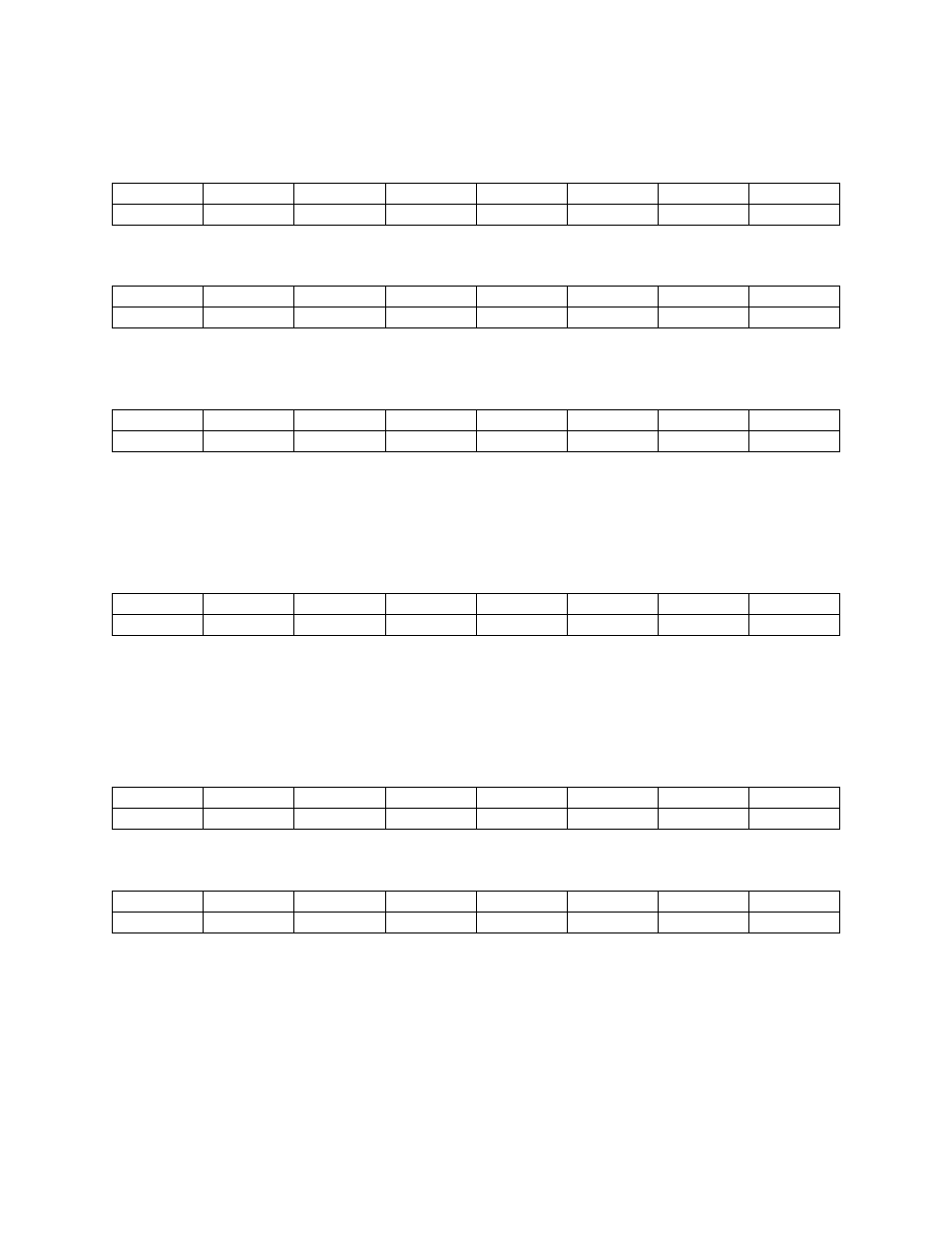
6.1.10 PACER CLOCK DATA & CONTROL REGISTERS
8254 COUNTER 0 DATA
BASE ADDRESS + Ch
D1
D2
D3
D4
D5
D6
D7
D8
0
1
2
3
4
5
6
7
8254 COUNTER 1 DATA
BASE ADDRESS + Dh
D1
D2
D3
D4
D5
D6
D7
D8
0
1
2
3
4
5
6
7
8254 COUNTER 2 DATA
BASE ADDRESS + Eh
D1
D2
D3
D4
D5
D6
D7
D8
0
1
2
3
4
5
6
7
The three 8254 counter/timer data registers can be written to and read from. Because each counter will
count as high as 64,535, it is clear that loading or reading the counter data must be a multi-step process.
The operation of the 8254 is explained in Intel 8254 data sheet.
8254 COUNTER CONTROL
BASE ADDRESS + Fh
D1
D2
D3
D4
D5
D6
D7
D8
0
1
2
3
4
5
6
7
This register controls the operation and loading/reading of the counters. The configuration of the 82C54
codes which control the chip is explained in the Intel 82C54 data sheet.
6.1.11 24-bit DIGITAL I/O REGISTERS (not applicable on -P5 versions)
PORT A DATA
BASE ADDRESS + 400h
D0
D1
D2
D3
D4
D5
D6
D7
0
1
2
3
4
5
6
7
PORT B DATA
BASE ADDRESS +401h
B0
B1
B2
B3
B4
B5
B6
B7
0
1
2
3
4
5
6
7
Ports A & B can be programmed as input or output. Each is written to and read from in bytes, although
for control and monitoring purposes the individual bits are used.
Bit set/reset and bit read functions require that unwanted bits be masked out of reads and ORed into
writes.
27