Measurement Computing CIO-DAS160x/1x User Manual
Page 28
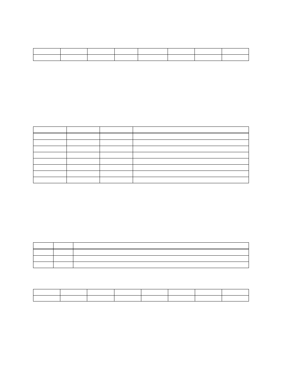
6.1.7
DMA, INTERRUPT & TRIGGER CONTROL
BASE ADDRESS + 9
TS0
TS1
DMA
X
IR0
IR1
IR2
INTE
0
1
2
3
4
5
6
7
A read and write register.
READ
INTE = 1, Interrupts are enabled. An interrupt generated will be placed on the PC bus interrupt level
selected by IR4, IR2 & IR1. INTE = 0, interrupts are disabled.
IR2, IR1, IR0 are bits in a binary number between 0 and 7 which map interrupts onto the PC bus interrupt
levels 2 to 7. Interrupts 0 and 1 cannot be asserted by the CIO-DAS1600.
Table 6-2. Interrupt Program Codes
7
1
1
1
6
0
1
1
5
1
0
1
4
0
0
1
3
1
1
0
2
0
1
0
None
1
0
0
None
0
0
0
INTERRUPT LEVEL
IR0
IR1
IR2
When DMA = 1, DMA transfers are enabled.
When DMA = 0, DMA transfers are disabled.
Note that this bit only allows the CIO-DAS1600 to assert a DMA request to the PC on the DMA request
level selected by the DMA switch on the CIO-DAS1600. Before this bit is set to 1, the PC's 8237 (or
appropriate) DMA controller chip must be set up.
TS1 & TS0 control the source of the A/D start conversion trigger according to Table 6-3 below.
Table 6-3. Source Codes for the A/D Start Conversion Trigger
Start on Pacer Clock Pulse (CTR 2 OUT, no external access)
1
1
Start on rising edge (Digital input 0, Pin 25)
0
1
Software triggered A/D only
X
0
TS0
TS1
6.1.8
PACER CLOCK CONTROL REGISTER
BASE ADDRESS + Ah
TRIG0
CTR0
X
X
BL0
BL1
BL2
BL3
0
1
2
3
4
5
6
7
Write only
24