Measurement Computing CIO-DAS160x/1x User Manual
Page 25
BASE ADDRESS +1
A/D 4
A/D 5
A/D 6
A/D 7
A/D 8
A/D 9
A/D 10
A/D 11
MSB
0
1
2
3
4
5
6
7
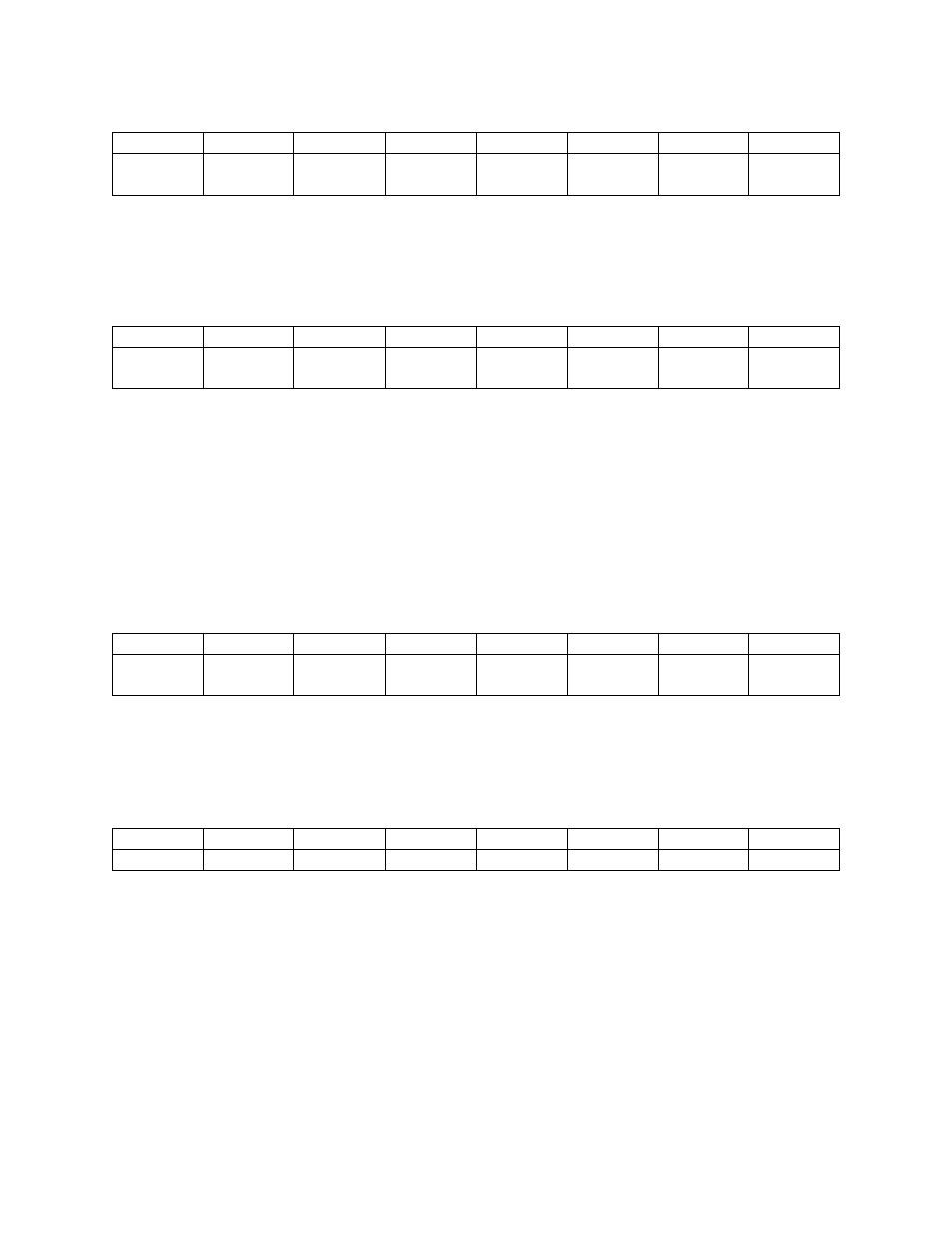
A Read-only register.
On read the most significant A/D byte is read.
6.1.2
A/D DATA & CHANNEL REGISTERS (CIO-DAS1602/16)
BASE ADDRESS
A/D 0
LSB
A/D 1
A/D 2
A/D 3
A/D 4
A/D 5
A/D 6
A/D 7
0
1
2
3
4
5
6
7
A read/write register.
READ
On read, it contains the least significant eight digits of the analog input data.
These eight bits of analog input data must be combined with the eight bits of analog input data in
BASE + 1, to form a complete 16-bit number. The data format is 0 =
−FS; 65,535 = +FS.
WRITE
Writing any data to the register causes an immediate A/D conversion
.
BASE ADDRESS +1
A/D 8
A/D 9
A/D 10
A/D 11
A/D 12
A/D 13
A/D 14
A/D 15
MSB
0
1
2
3
4
5
6
7
A Read-only register.
On read the most significant A/D byte is read
.
6.1.3
CHANNEL MUX SCAN LIMITS REGISTER
BASE ADDRESS +2
CH L0
CH L1
CH L2
CH L3
CH H0
CH H1
CH H2
CH H3
0
1
2
3
4
5
6
7
A read and write register.
READ
The current channel scan limits are read as one byte. The high channel number scan limit is in the most
significant four bits. The low channel scan limit is in the least significant four bits.
WRITE
The channel scan limits desired are written as one byte. The high channel number scan limit is in the
most significant four bits. The low channel scan limit is in the least significant four bits.
NOTE
Every write to this register sets the current A/D channel MUX setting to the number in
bits 0-3 and resets the FIFO. See BASE + 8.
21