Measurement Computing CIO-DAS160x/1x User Manual
Page 24
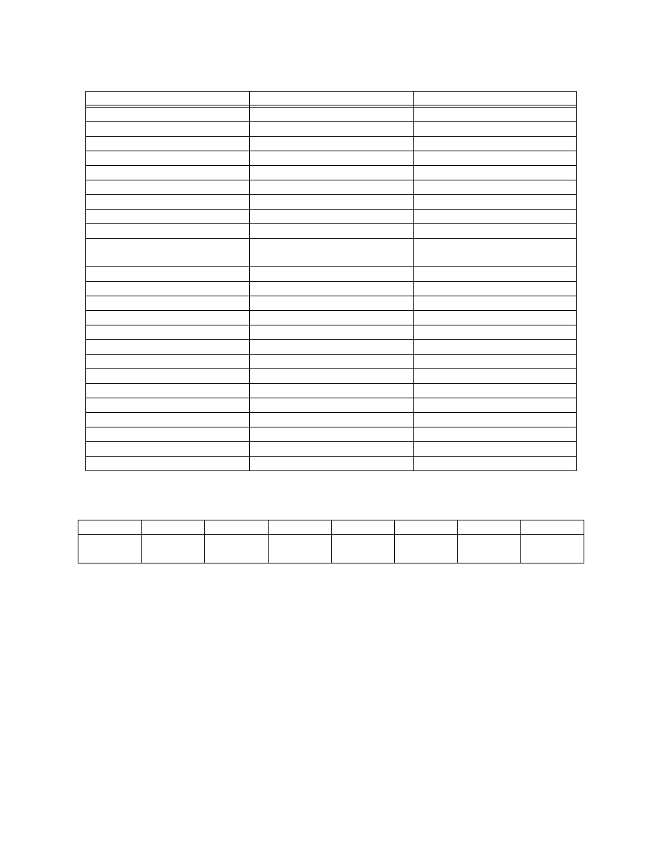
Table 6-1. Register Map
None
Status of extended features
BASE + 407h
DAS 1600 Enable/Disable
None
BASE + 406h
Burst Mode Enable/Disable
None
BASE + 405h
Conversion Enable/Disable
None
BASE + 404h
Configure 8255, n/a on -P5 ver.
None. No read back on 8255
BASE + 403h
Port C Output, n/a on -P5 ver.
Port C Input
BASE + 402h
Port B Output, n/a on -P5 ver.
Port B Input
BASE + 401h
Port A Output, n/a on -P5 ver.
Port A Input of 8255
BASE + 400h
Pacer Clock Control (8254)
None. No read back on 8254
BASE + Fh
CTR 2 Data - A/D Pacer
CTR 2 Data - A/D Pacer Clock
BASE + Eh
CTR 1 Data - A/D Pacer
CTR 1 Data - A/D Pacer Clock
BASE + Dh
Counter 0 Data
Counter 0 Data
BASE + Ch
PGA Control/DT reset
PGA gain
BASE + Bh
Burst Length/pacer clk cntrl
none
BASE + Ah
Set DMA, INT etc
DMA, Interrupt & Trigger
Control
BASE + 9
Clear Interrupt
Status EOC, UNI/BIP etc.
BASE + 8
D/A 1 Most Significant bits
None
BASE + 7
D/A 1 Least Significant bits
None
BASE + 6
D/A 0 Most Significant bits
None
BASE + 5
D/A 0 Least Significant bits
None
BASE + 4
Digital 4 Bit Output
Digital 4-Bit Input
BASE + 3
Channel MUX / FIFO reset
Channel MUX
BASE + 2
None
A/D Data (Most significant)
BASE + 1
Start A/D Conversion
A/D Data (Least significant)
BASE
WRITE FUNCTION
READ FUNCTION
ADDRESS
6.1.1
A/D DATA & CHANNEL REGISTERS (CIO-DAS1600/12)
BASE ADDRESS +0
CH0
CH1
CH2
CH3
A/D 0
LSB
A/D 1
A/D 2
A/D 3
0
1
2
3
4
5
6
7
A read/write register.
READ
On read, it contains two types of data. The least significant four digits of the analog input data and the
channel number from which the current data was taken.
These four bits of analog input data must be combined with the eight bits of analog input data in BASE +
1 to form a complete 12-bit number. The data format is 0 =
−FS; 4095 = +FS.
The channel number is binary. If the current channel is 5, bits CH2 and CH0 are high, CH3 and CH1 are
low.
WRITE
Writing any data to the register causes an immediate A/D conversion.
20