Voltage divider jumpers j30 and j32 – Measurement Computing SC-1608 Series User Manual
Page 21
SC-1608 Series User's Guide
Functional Details
21
When set to position 1-2 (not shown in the diagram), the same voltage readback functionality is available using
J35 pin 25 and non-isolated analog input CH8 (pin 13). The signal is non-isolated in this configuration, as
AOUT0 is no longer connected to AIN CH8.
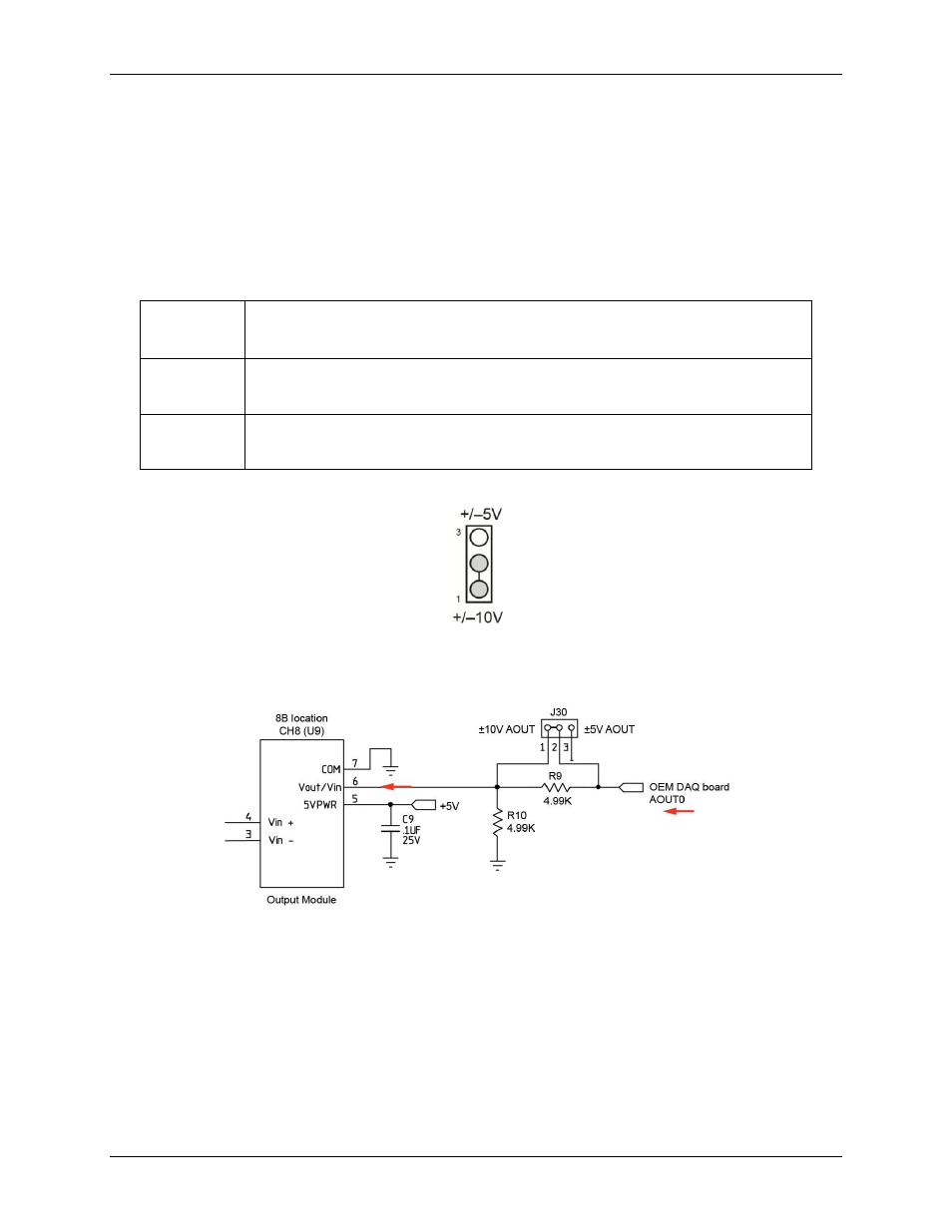
Voltage divider jumpers J30 and J32
These jumpers are used to scale the OEM DAQ board AOUTx channel output voltage range to match the
voltage input range of an analog output module installed at CH8 (U9) or CH9 (U10).
The following tables list the configuration settings of jumpers J30 and J32.
Jumper J30 (location CH8) and J32 (location CH9) configuration
J30/32
jumper
position
Function
1-2
(default)
J30: OEM DAQ board channel AOUT0 outputs ±10V output (default)
J32: OEM DAQ board channel AOUT1 outputs ±10V output (default)
2-3
J30: OEM DAQ board channel AOUT0 ±10V output is scaled to ±5V
OEM DAQ board channel AOUT1 ±10V output is scaled to ±5V
Figure 12 shows jumper 30 and 32 set for its default configuration.
Figure 12. Jumper J30 and J32 default configuration (output ±10V)
Figure 13 illustrates the connection flow when an output module is installed in module location CH8, and
jumper J30 is set for position 2-3.
Figure 13. J30/J32 voltage divider schematic
In this scenario, the OEM DAQ board channel AOUT0 is configured to output ±10V.
If an 8B output module is installed that has an output range of ±5V or 0-5 V, configure this jumper for position
2-3 to scale the voltage output by the OEM DAQ board AOUT0 channel to ±5V.