Altera Nios Development Board User Manual
Page 47
Altera Corporation
A–3
July 2005
Note to
(1)
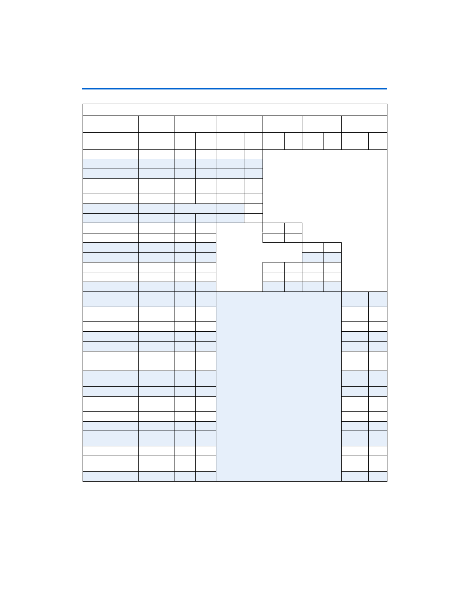
This pin is NC for AM29LV128M but is provided for compatible devices that have the active pin A23.
Pin
Name
Pin #
Pin
Name
Pin #
Pin
Name
Pin #
Pin
Name
Pin #
Pin
Name
Pin #
FLASH_CS_n
Chip Select
IO
AE4
CE_n
32
FLASH_OE-N
Read Enable
IO
AB9
OE_n
34
FLASH_RW-N
Write Enable
IO
AD6
WE_n
13
FLASH_WP_N
Write
Protect/ACC
IO
Y6
WE_n.ACC
16
FLASH _BYTE_N
Byte Enable
IO
AB11
BYTE_n
53
FLASH_RESET_N
Reset
Reset_n
14
FLASH_RY-BY_N
Ready/Busy
IO
AE6
RY/BY_n
17
SRAM_BE_N0
Byte Enable 0
IO
K20
BE0#
39
SRAM_BE_N1
Byte Enable 1
IO
K19
BE1#
40
SRAM_BE_N2
Byte Enable 2
IO
K22
BE2#
39
SRAM_BE_N3
Byte Enable 3
IO
K21
BE3#
40
SRAM_CS_N
Chip Select
IO
J19
CS_n
6
CS_n
6
SRAM_OE_N
Read Enable
IO
J22
OE_n
41
OE_n
41
SRAM_WE_N
Write Enable
IO
J21
WE_n
17
WE_n
17
ENET_ADS_N
Address
Strobe
IO
AD2
ADS#
37
ENET_AEN
Address
Enable
IO
AF10
AEN
41
ENET_BE_N0
Byte Enable 0
IO
AD8
BE0#
94
ENET_BE_N1
Byte Enable 1
IO
AF9
BE1#
95
ENET_BE_N2
Byte Enable 2
IO
Y11
BE2#
96
ENET_BE_N3
Byte Enable 3
IO
W12
BE3#
97
ENET_CYCLE_N
Bus Cycle
IO
AC9
CYCLE#
35
ENET_DATACS_N
Data Chip
Select
IO
Y12
DATACS
#
34
ENET_INTRQ0
Interrupt
IO
AD11
INTRO
29
ENET_IOCHRDY
IO Char
Ready
IO
AD1
ARDY
38
ENET_IOR_N
Read
IO
AC10
RD#
31
ENET_IOW_N
Write
IO
AE11
WR#
32
ENET_LCLK
Local Bus
Clock
IO
W11
LCLK
42
ENET_LDEV_N
Local Device
IO
Y7
LDEV#
45
ENET_RDYRTN_N
Ready Return
IO
V12
RDYRTN
#
46
ENET_W_R_N
Write/Read
IO
AC8
W/R#
36
Table A–9. Shared Bus Table (Part 3 of 3)
NET Name
NET
Description
PLD (U60)
Flash (U5)
SRAM (U35)
SRAM (U36)
Ethernet (U4)