Clock circuitry – Altera Nios Development Board User Manual
Page 42
2–34
Altera
Corporation
Nios Development Board Reference Manual, Stratix II Edition
July 2005
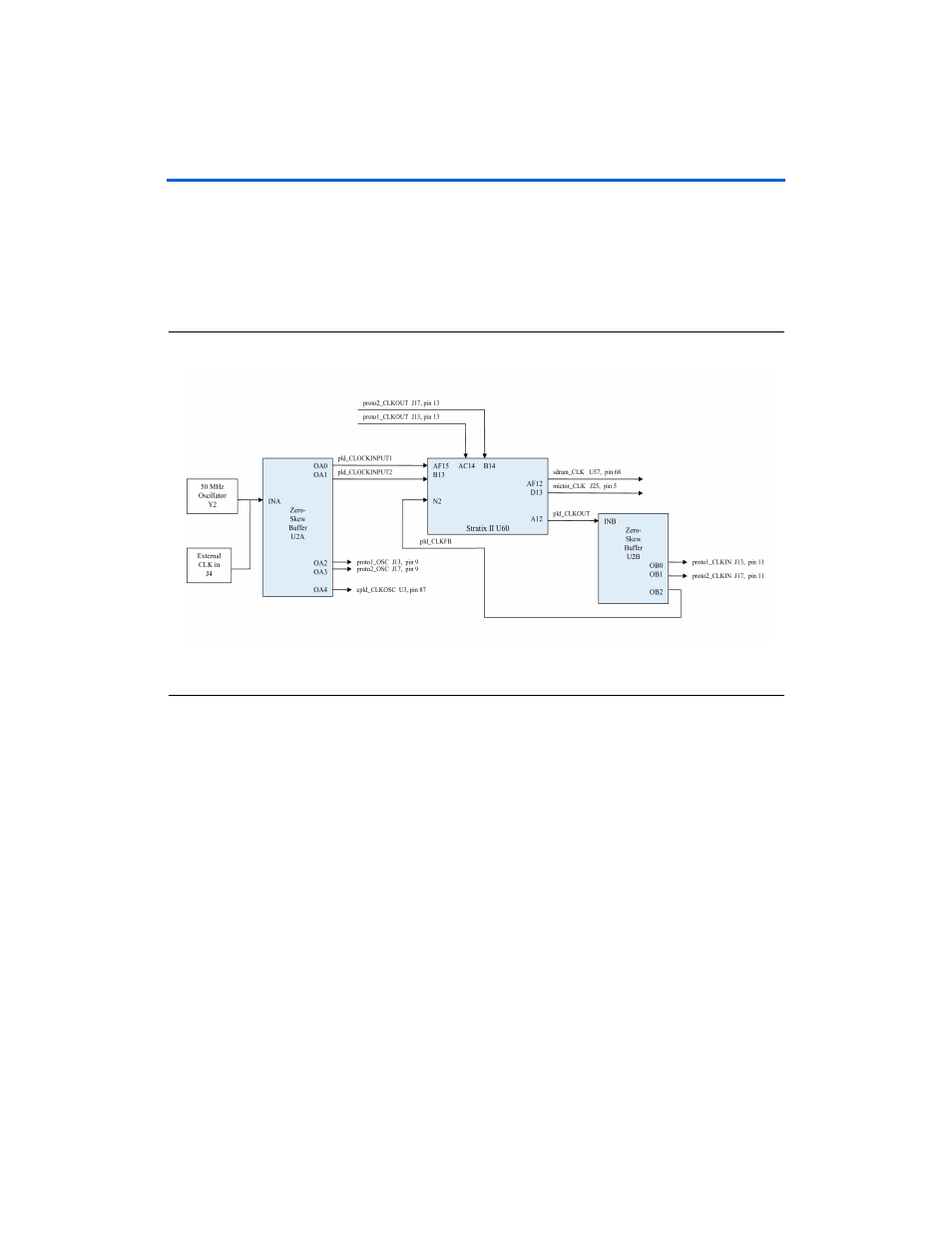
Clock Circuitry
Clock Circuitry
The Nios development board includes a 50 MHz free-running oscillator
(Y2) and a zero-skew, point-to-point clock distribution network that
drives the Stratix II FPGA (U60), the EPM7128AE configuration controller
device (U3), and pins on the PROTO1 & PROTO2 connectors. The zero-
skew buffer (U2) distributes both the free-running 50 MHz clock and a
clock output from one of the FPGA's internal PLLs. See
.
Figure 2–21. Clock Circuitry
Note to
(1)
An external clock can be enabled by stuffing location R15 with a 49.9 ohm 0603 resistor and stuffing location R13
with a 330 ohm 0603 resistor.
The Stratix II FPGA receives clock input from buffer U2, and from the
PROTO1 and PROTO2 connectors, as follows:
■
The buffer U2 drives the Stratix II pins AF15 (CLK4p) and B13
(CLK12p).
■
The proto1_CLKOUT net (J13, pin 13) drives the Stratix II pin AC14
(CLK5p).
■
The proto2_CLKOUT net (J17, pin 13) drives the Stratix II pin B14
(CLK3p).
The FPGA can synthesize new clock signals internally using on-chip
PLLs, and drive the clocks to various components on the board. As shown
in
, the clock circuitry allows the Stratix II FPGA to:
■
Drive the SDRAM chip (U57) via pin AF12, driven by on-chip PLL6.
■
Drive the Mictor connector (J25) clock via pin D13, driven by on-chip
PLL5.