Compactflash connector (con3), Compactflash connector (con3) –20 – Altera Nios Development Board User Manual
Page 28
2–20
Altera
Corporation
Nios Development Board Reference Manual, Stratix II Edition
July 2005
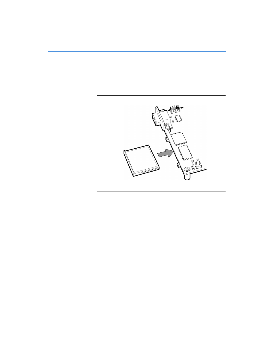
CompactFlash Connector (CON3)
CompactFlash
Connector
(CON3)
The CompactFlash connector header (CON3) enables hardware designs
to access a CompactFlash card. See
. The following two access
modes are supported:
■
ATA (hot swappable mode)
■
IDE (IDE hard disk mode)
Figure 2–11. CompactFlash Connector
Most pins of CON3 connect to I/O pins on the FPGA. The following pins
have special connections:
■
Pin 13 of CON3 (VCC) is driven by a power MOSFET that is
controlled by an FPGA I/O pin. This allows the FPGA to control
power to the CompactFlash card for the IDE connection mode.
■
Pin 26 of CON3 (-CD1) is pulled up to 5V through a 10 Kohm resistor.
This signal is used to detect the presence of a CompactFlash card;
when the card is not present, the signal is pulled high through the
pull-up resistor.
■
Pin 41 of CON3 (RESET) is pulled up to 5V through a 10 Kohm
resistor, and is controlled by the EPM7128AE configuration
controller. The FPGA can cause the configuration controller to assert
RESET, but the FPGA does not drive this signal directly.
1
The CompactFlash connector shares several Stratix II I/O pins
with expansion prototype connector PROTO1. See
Prototype Connectors (PROTO1 & PROTO2)” on page 2–15
for
details on PROTO1.