Flash, Flash –45 – Altera Cyclone IV GX FPGA Development Board User Manual
Page 53
Chapter 2: Board Components
2–45
Memory
May 2013
Altera Corporation
Cyclone IV GX FPGA Development Board
Reference Manual
Flash
The flash interface consists of a single synchronous flash memory device, providing
64 MB of memory with a 16-bit data bus. This device is part of the shared FSM bus
which connects to the flash memory, SRAM, LCD, and MAX II CPLD EPM2210
System Controller.
This 16-bit data memory interface can sustain burst read operations at up to 52 MHz
for a throughput of 832 Mbps. The write performance is 125
μs for a single word and
440
μs for a 32-word buffer. The erase time is 400 ms for a 32 K parameter block and
1200 ms for a 128 K main block.
f
For more information about the flash memory map storage, refer to th
lists the flash pin assignments, signal names, and functions. The signal
names and types are relative to the Cyclone IV GX device in terms of I/O setting and
direction.
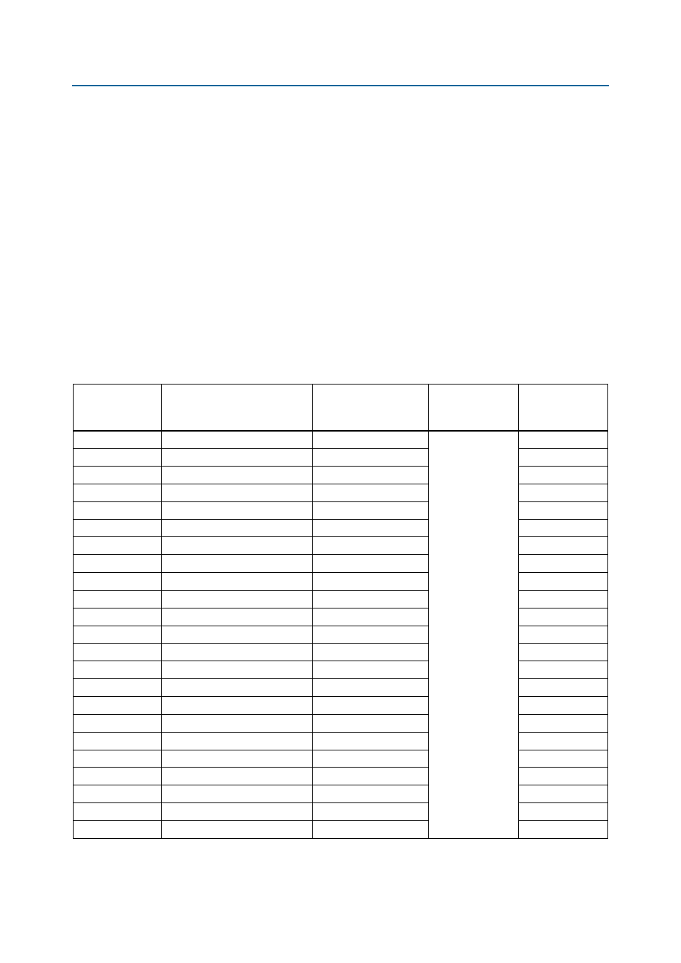
Table 2–42. Flash Pin Assignments, Schematic Signal Names, and Functions (Part 1 of 2)
Board Reference
Description
Schematic Signal Name
I/O Standard
Cyclone IV GX
Device
Pin Number
U6.F6
Address valid
FLASH_ADVn
1.8-V
F24
U6.B4
Chip enable
FLASH_CEn
E25
U6.E6
Clock
FLASH_CLK
Y21
U6.F8
Output enable
FSM_OEn
F7
U6.F7
Ready
FLASH_RDYBSYn
B7
U6.D4
Reset
FLASH_RESETn
A28
U6.G8
Write enable
FSM_WEn
C13
U6.C6
Write protect
FLASH_WPn
Pulled high
U6.A1
Address bus
FSM_A1
AD6
U6.B1
Address bus
FSM_A2
AK29
U6.C1
Address bus
FSM_A3
AA21
U6.D1
Address bus
FSM_A4
AG25
U6.D2
Address bus
FSM_A5
AH5
U6.A2
Address bus
FSM_A6
AH27
U6.C2
Address bus
FSM_A7
AJ12
U6.A3
Address bus
FSM_A8
AF16
U6.B3
Address bus
FSM_A9
AH20
U6.C3
Address bus
FSM_A10
AK23
U6.D3
Address bus
FSM_A11
AH17
U6.C4
Address bus
FSM_A12
AB21
U6.A5
Address bus
FSM_A13
AF19
U6.B5
Address bus
FSM_A14
AF12
U6.C5
Address bus
FSM_A15
AG27