Configuration push buttons, Clock circuitry, Configuration push buttons –20 – Altera Cyclone IV GX FPGA Development Board User Manual
Page 28: Clock circuitry –20
2–20
Chapter 2: Board Components
Clock Circuitry
Cyclone IV GX FPGA Development Board
May 2013
Altera Corporation
Reference Manual
Configuration Push Buttons
The program load push button (S8), is an input to the MAX
II CPLD EPM2210 System
Controller. The push button forces a reconfiguration of the FPGA from flash memory.
The location in the flash memory is based on the board settings DIP switch’s
position. Valid settings include FACTORY or USER.
The program select push button (S7), toggles the program LEDs (D3, D4) sequence.
Refer to
for the LED sequence definitions.
lists the configuration push buttons component reference and
manufacturing information.
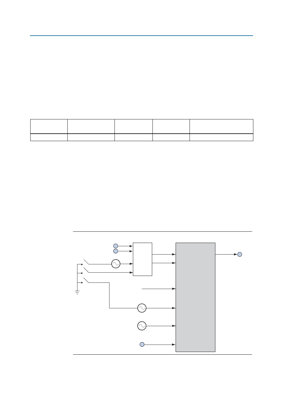
Clock Circuitry
The dedicated clock inputs are located on the top bank 8B and bottom bank 3B of the
Cyclone IV GX device. An on-board programmable oscillator or a bench supply clock
can be distributed to these dedicated clock inputs. The clock going to bank 3B is a
dedicated clock input for 3G applications.
The non-dedicated clocks are located on banks 3A and 8A of the Cyclone IV GX
device. The PCIe reference clock is on bank 3A while the 125-MHz clock is on bank
8A.
shows the Cyclone IV GX FPGA development board’s transceiver clock
structure.
Table 2–17. Configuration Push Buttons Component Reference and Manufacturing Information
Board Reference
Description
Manufacturer
Manufacturer
Part Number
Manufacturer Website
S7, S8
Push buttons
Panasonic
EVQPAC07K
Figure 2–5. Cyclone IV GX FPGA Development Board Transceiver Clock Structure
CLKIN SMA (J10)
ICS8543
CLKBUF
(U25)
FPGA
(U10)
CLKOUT SMA (J9)
PCI Express Reference Clock
125-MHz Oscillator (X2)
50-MHz Oscillator (X3)
LVPECL Input Clock (J11, J12)
100-MHz Oscillator (X4)
CLKA_SEL
CLK125_EN
CLKA_EN
Bank 8
Bank 4
Bank 8A
Bank 3A
Bank 8B
Bank 3B
Bank 4