Lcd –24 – Altera Cyclone IV GX FPGA Development Board User Manual
Page 32
2–24
Chapter 2: Board Components
General User Input/Output
Cyclone IV GX FPGA Development Board
May 2013
Altera Corporation
Reference Manual
lists the user-defined LED component reference and the manufacturing
information.
LCD
The development board contains a single 14-pin 0.1" pitch dual-row header that
interfaces to a 16 character × 2 line Lumex LCD display. The LCD has a 14-pin
receptacle that mounts directly to the board's 14-pin header, so it can be easily
removed for access to components under the display. You can also use the header for
debugging or other purposes.
summarizes the LCD pin assignments. The signal names and directions are
relative to the Cyclone IV GX FPGA.
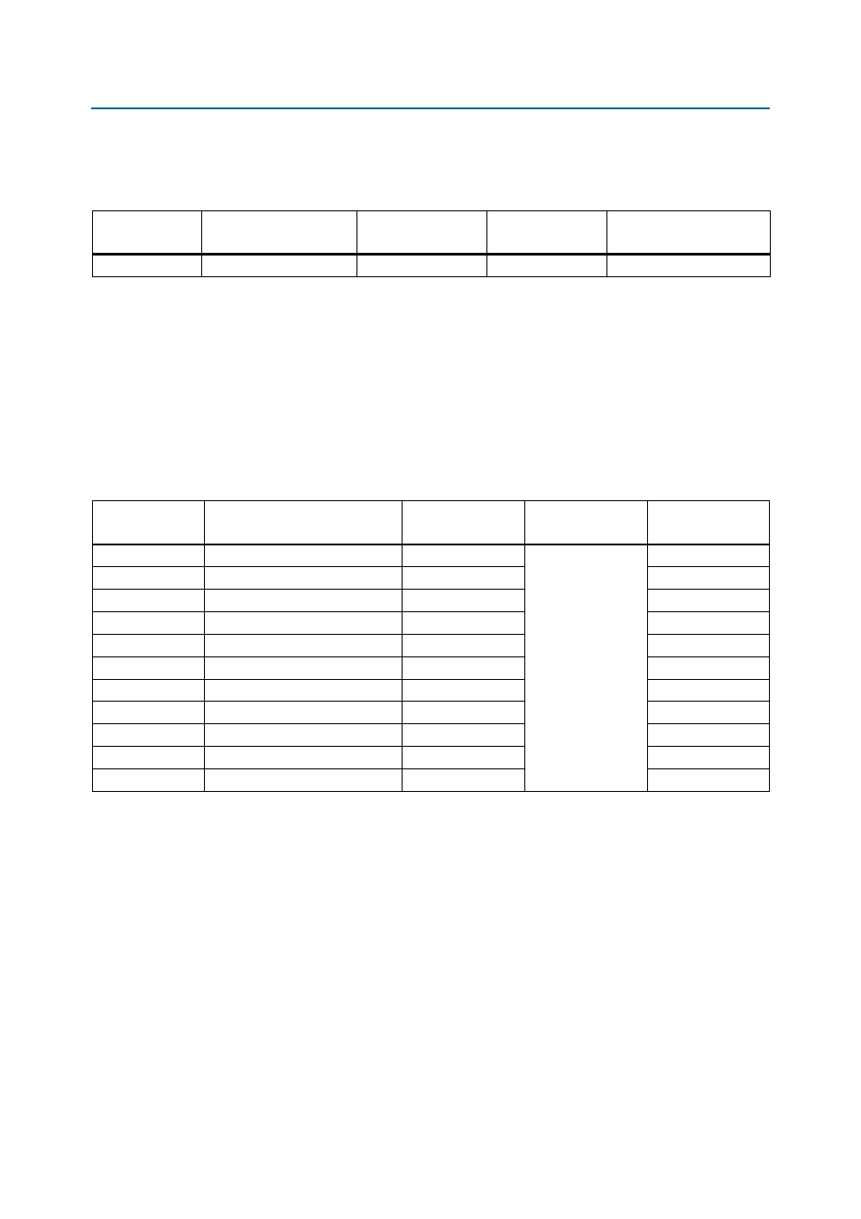
Table 2–25. User-Defined DIP Switch Component Reference and Manufacturing Information
Board Reference
Device Description
Manufacturer
Manufacturer
Part Number
Manufacturer Website
SW2
Eight-Position DIP switch
C & K Components
TDA08H0SB1
Table 2–26. LCD Pin Assignments, Schematic Signal Names, and Functions
Board Reference
Description
Schematic Signal
Name
I/O Standard
Cyclone IV GX
Device Pin Number
J13.4
LCD data or command select
LCD_D_Cn
2.5-V CMOS
D5
J13.5
LCD write enable
LCD_WEn
E6
J13.6
LCD chip select
LCD_CSn
C3
J13.7
LCD data bus
LCD_DATA0
C15
J13.8
LCD data bus
LCD_DATA1
F9
J13.9
LCD data bus
LCD_DATA2
D7
J13.10
LCD data bus
LCD_DATA3
E21
J13.11
LCD data bus
LCD_DATA4
C27
J13.12
LCD data bus
LCD_DATA5
G13
J13.13
LCD data bus
LCD_DATA6
E10
J13.14
LCD data bus
LCD_DATA7
F16
Note to
:
(1) All signals are translated from 1.8-V to 2.5-V using a dual/quad low-voltage level translators except for LCD_DATA4, which connects directly to
the PLL4_CLKOUTn pin of the Cyclone IV GX FPGA.