Altera Cyclone IV GX FPGA Development Board User Manual
Page 50
2–42
Chapter 2: Board Components
Memory
Cyclone IV GX FPGA Development Board
May 2013
Altera Corporation
Reference Manual
lists the DDR2 component reference and manufacturing information.
U19.C8
Data bus byte lane 1
DDR2B_DQ8
1.8-V SSTL Class I
AJ10
U19.C2
Data bus byte lane 1
DDR2B_DQ9
AG9
U19.D7
Data bus byte lane 1
DDR2B_DQ10
AG13
U19.D3
Data bus byte lane 1
DDR2B_DQ11
AH11
U19.D1
Data bus byte lane 1
DDR2B_DQ12
AG10
U19.D9
Data bus byte lane 1
DDR2B_DQ13
AH12
U19.B1
Data bus byte lane 1
DDR2B_DQ14
AE12
U19.B9
Data bus byte lane 1
DDR2B_DQ15
AE13
U19.B3
Write mask byte lane 1
DDR2B_DM1
AJ6
U19.B7
Data strobe byte lane 1
DDR2B_DQS1
AH13
U17.G8
Data bus byte lane 2
DDR2B_DQ16
AA15
U17.G2
Data bus byte lane 2
DDR2B_DQ17
AK11
U17.H7
Data bus byte lane 2
DDR2B_DQ18
AH15
U17.H3
Data bus byte lane 2
DDR2B_DQ19
AE14
U17.H1
Data bus byte lane 2
DDR2B_DQ20
AK8
U17.H9
Data bus byte lane 2
DDR2B_DQ21
AH16
U17.F1
Data bus byte lane 2
DDR2B_DQ22
AJ7
U17.F9
Data bus byte lane 2
DDR2B_DQ23
AB16
U17.F3
Write mask byte lane 2
DDR2B_DM2
AH18
U17.F7
Data strobe byte lane 2
DDR2B_DQS2
AF15
U17.C8
Data bus byte lane 3
DDR2B_DQ24
AH18
U17.C2
Data bus byte lane 3
DDR2B_DQ25
AK17
U17.D7
Data bus byte lane 3
DDR2B_DQ26
AJ18
U17.D3
Data bus byte lane 3
DDR2B_DQ27
AK18
U17.D1
Data bus byte lane 3
DDR2B_DQ28
AK15
U17.D9
Data bus byte lane 3
DDR2B_DQ29
AE18
U17.B1
Data bus byte lane 3
DDR2B_DQ30
AJ15
U17.B9
Data bus byte lane 3
DDR2B_DQ31
AH19
U17.B3
Write mask byte lane 3
DDR2B_DM3
Y17
U17.B7
Data strobe P byte lane 3
DDR2B_DQS3
AA17
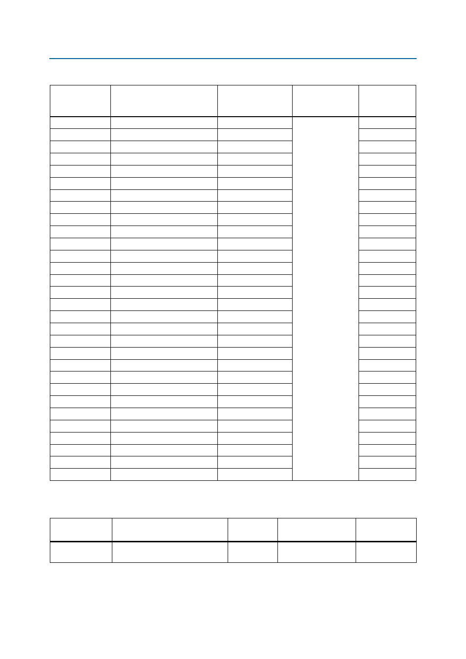
Table 2–38. DDR2 SDRAM Bottom Port Pin Assignments, Signal Names and Functions (Part 2 of 2)
Board Reference
Description
Schematic Signal
Name
I/O Standard
Cyclone IV GX
Device
Pin Number
Table 2–39. DDR2 Component Reference and Manufacturing Information
Board Reference
Description
Manufacturer
Manufacturing
Part Number
Manufacturer
Website
U8, U15, U17, U19
16 M × 16-bit × 4 banks, 533Mbps,
CL4
Micron
MT47H16M16BG-37E:B