Altera Cyclone IV GX FPGA Development Board User Manual
Page 38
2–30
Chapter 2: Board Components
Components and Transceiver Interfaces
Cyclone IV GX FPGA Development Board
May 2013
Altera Corporation
Reference Manual
The HSMC connector has a total of 172 pins, including 120 signal pins, 39 power pins,
and 13 ground pins. The ground pins are located between the two rows of signal and
power pins, acting both as a shield and a reference. The HSMC host connector is
based on the 0.5 mm-pitch QSH/QTH family of high-speed, board-to-board
connectors from Samtec. There are three banks in this connector. Bank 1 has every
third pin removed as done in the QSH-DP/QTH-DP series. Bank 2 and bank 3 have
all the pins populated as done in the QSH/QTH series.
The HSMC port A interface has programmable bi-directional I/O pins that can be
used as 2.5-V LVCMOS, which is 3.3-V LVTTL-compatible. These pins can also be
used as various differential I/O standards including, but not limited to, LVDS,
mini-LVDS, and RSDS with up to 17 full-duplex channels. The HSMC port B interface
is translated from 1.8 V (on the FPGA) to 2.5 V (on the HSMC connector) using a
bidirectional voltage translator.
1
As noted in the
manual, LVDS and
single-ended I/O standards are only guaranteed to function when mixed according to
either the generic single-ended pin-out or generic differential pin-out.
lists the HSMC port A interface pin assignments, signal names, and
functions.
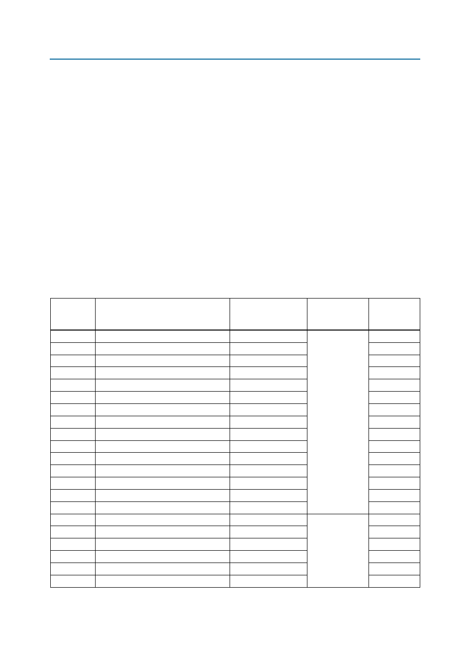
Table 2–33. HSMC Port A Pin Assignments, Schematic Signal Names, and Functions (Part 1 of 4)
Board
Reference
Description
Schematic Signal
Name
I/O Standard
Cyclone IV GX
Device
Pin Number
J1.17
Transceiver TX bit 3
HSMA_TX_P3
1.5 V
H4
J1.19
Transceiver TX bit 3n
HSMA_TX_N3
H3
J1.18
Transceiver RX bit 3
HSMA_RX_P3
J2
J1.20
Transceiver RX bit 3n
HSMA_RX_N3
J1
J1.21
Transceiver TX bit 2
HSMA_TX_P2
K4
J1.23
Transceiver TX bit 2n
HSMA_TX_N2
K3
J1.22
Transceiver RX bit 2
HSMA_RX_P2
L2
J1.24
Transceiver RX bit 2n
HSMA_RX_N2
L1
J1.25
Transceiver TX bit 1
HSMA_TX_P1
M4
J1.27
Transceiver TX bit 1n
HSMA_TX_N1
M3
J1.26
Transceiver RX bit 1
HSMA_RX_P1
N2
J1.28
Transceiver RX bit 1n
HSMA_RX_N1
N1
J1.29
Transceiver TX bit 0
HSMA_TX_P0
P4
J1.31
Transceiver TX bit 0n
HSMA_TX_N0
P3
J1.30
Transceiver RX bit 0
HSMA_RX_P0
R2
J1.32
Transceiver RX bit 0n
HSMA_RX_N0
2.5-V
R1
J1.33
Management serial data
HSMA_T_SDA
C25
J1.34
Management serial clock
HSMA_T_SCL
B24
J1.35
JTAG clock signal
JTAG_TCK
F2
J1.36
JTAG mode select signal
JTAG_TMS
E1
J1.37
JTAG data output
HSMA_JTAG_TDO
—