I/o resources, I/o resources –6 – Altera Transceiver Signal Integrity Development Kit, Stratix IV GT Edition User Manual
Page 16
2–6
Chapter 2: Board Components
Featured Device: Stratix IV GT Device
Transceiver Signal Integrity Development Kit,
November 2011
Altera Corporation
Stratix IV GT Edition Reference Manual
lists the features of the Stratix IV GT EP4S100G2F40I1N device.
lists the Stratix IV GT component reference and manufacturing
information.
I/O Resources
shows the bank organization and I/O count for the EP4S100G2F40I1N
device in the 1517-pin FBGA package.
Table 2–2. Stratix IV GT Device EP4S100G2F40I1N Features
ALMs
Equivalent
LEs
M9K
RAM
Blocks
M144K
Blocks
Total
RAM
bits
DSP
Blocks
18-bit × 18-bit
Multipliers
PLLs
Maximum
User I/O pins
Package
Type
91,200
228,000
1,235
22
17,133
161
1,288
8
636
1517-pin
FBGA
Table 2–3. Stratix IV GT Device Component Reference and Manufacturing Information
Board Reference
Description
Manufacturer
Manufacturing
Part Number
Manufacturer
Website
U33
Stratix IV GT
Altera
Corporation
EP4S100G2F40I1N
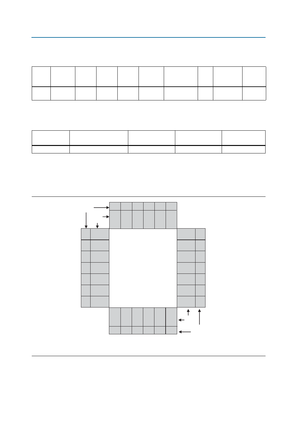
Figure 2–2. Stratix IV GT Device I/O Bank Diagram
Note to
(1) There are two additional PMA-only transceiver channels in each transceiver bank.
B
ank
8B
24
B
ank
7A
40
B
ank
7B
24
B
ank
7C
32
22 Bank 1C
23 Bank 2C
24
B
ank
3B
40
B
ank
4A
24
B
ank
4B
32
B
ank
4C
Bank 6C 23
Bank 5C 23
46 Bank 2A
B
ank
8C
32
B
ank
8A
40
32
B
ank
3C
40
B
ank
3A
Bank 5A 46
Bank 6A 44
Bank
Name
Number
of I/Os
Bank
Name
Number
of I/Os
43 Bank 1A
Bank
GXBL2
Bank
GXBL1
Bank
GXBL0
4 (1)
Bank
GXBR2
Bank
GXBR1
Bank
GXBR0
4 (1)
4 (1)
4 (1)
4 (1)
4 (1)
EP4S40G2
EP4S40G5
EP4S100G2
EP4S100G5