Altera Transceiver Signal Integrity Development Kit, Stratix IV GT Edition User Manual
Page 14
2–4
Chapter 2: Board Components
Board Overview
Transceiver Signal Integrity Development Kit,
November 2011
Altera Corporation
Stratix IV GT Edition Reference Manual
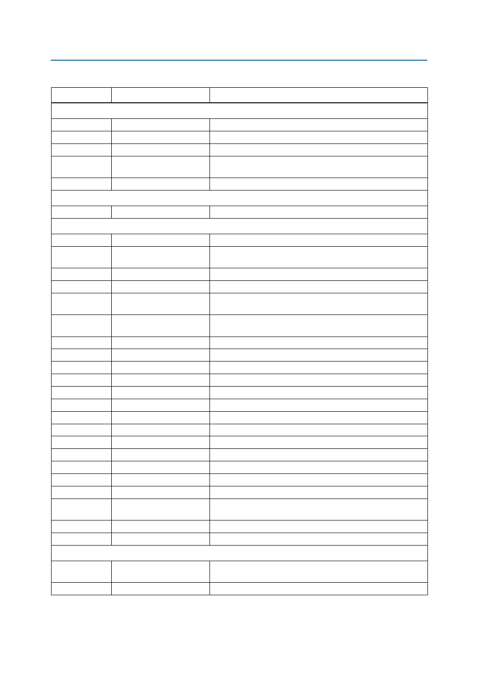
General User Input and Output
SW7
Bank of 8 user DIP switches
User DIP switches.
SW10–SW15
Bank of 6 user push buttons
User push buttons switches.
D8–D15
Bank of 8 user LEDs
User LEDs.
J25
General purpose user I/O
header field
Four user I/Os brought out to a 0.1 inch header field.
J24
LCD interface header
Header for interfacing a 16 character × 2 line LCD.
Memory Devices
U39
Flash memory
Numonyx 48F4400P0VB00, 512-Mb flash memory.
Components and Interfaces
CN1
USB Type-B connector
USB interface for embedded USB-Blaster.
U17
MAX II CPLD
Altera EPM7064AETC44 MAX II CPLD device for embedded
USB-Blaster circuitry.
J68
Ethernet RJ45 jack
Halo HFJ11-1G02E RJ45 Ethernet jack with integrated magnetic.
U40
10/100/1000 Ethernet PHY
Marvell 88E1111 triple speed Ethernet PHY.
J70
GXB0 transmit channel 0-5
Transceiver GXB0 transmit channel 0-5 connected to a backplane
connector.
J71
GXB0 receive channel 0-5
Transceiver GXB0 receive channel 0-5 connected to a backplane
connector.
J39, J41
GXB1 transmit channel 0
Transceiver GXB1 transmit channel 0 connected to SMA.
J43, J45
GXB1 transmit channel 1
Transceiver GXB1 transmit channel 1 connected to SMA.
J55, J57
GXB1 transmit channel 2
Transceiver GXB1 transmit channel 2 connected to SMA.
J59, J61
GXB1 transmit channel 3
Transceiver GXB1 transmit channel 3 connected to SMA.
J38, J40
GXB1 receive channel 0
Transceiver GXB1 receive channel 0 connected to SMA.
J42, J44
GXB1 receive channel 1
Transceiver GXB1 receive channel 1 connected to SMA.
J54, J56
GXB1 receive channel 2
Transceiver GXB1 receive channel 2 connected to SMA.
J58, J60
GXB1 receive channel 3
Transceiver GXB1 receive channel 3 connected to SMA.
J34, J36
GXB2 transmit channel 0
Transceiver GXB2 transmit channel 0 connected to SMA.
J30, J32
GXB2 receive channel 0
Transceiver GXB2 receive channel 0 connected to SMA.
J31, J33
GXB2 transmit channel 1
Transceiver GXB2 transmit channel 1 connected to SMA.
J35, J37
GXB2 receive channel 1
Transceiver GXB2 receive channel 1 connected to SMA.
J12
Fan power connector
Power connector for 5-V DC fan sink.
J64
Fan control jumper
Jumper to select whether the fan is always on or automatically
controlled by the FPGA.
SW8
Reset push button
Board reset push button.
SW9
CPU reset push button
CPU reset push button.
Power
J1
Power Input Jack
14-V – 20-V DC female input power jack. Accepts 2.5-mm male
center-positive barrel from supplied 16-V DC power supply.
SW1
Power switch
Switch to power on/off the board.
Table 2–1. Stratix IV GT Transceiver Signal Integrity Development Board Components (Part 3 of 4)
Board Reference
Type
Description