Spectrum Controls 1746sc-NI8u User Manual
Page 24
12
SLC 500
™
Universal Analog Input Module
JP9, JP10, and JP12
Setup
The NI8u module supports up to four RTD or resistance inputs on
channels 4 through 7. In order to properly support RTD or resistance
inputs, JP9, JP10, and JP12 have to be configured correctly. The
function of JP9 and JP10 is to define the input path for the channels 4
through 7. JP9 and JP10 are four pin headers toward the right side of
the board, looking at the primary side of the board with the terminal
block pointing up. JP12 is a three pin header on the very bottom
right hand corner, below JP11.
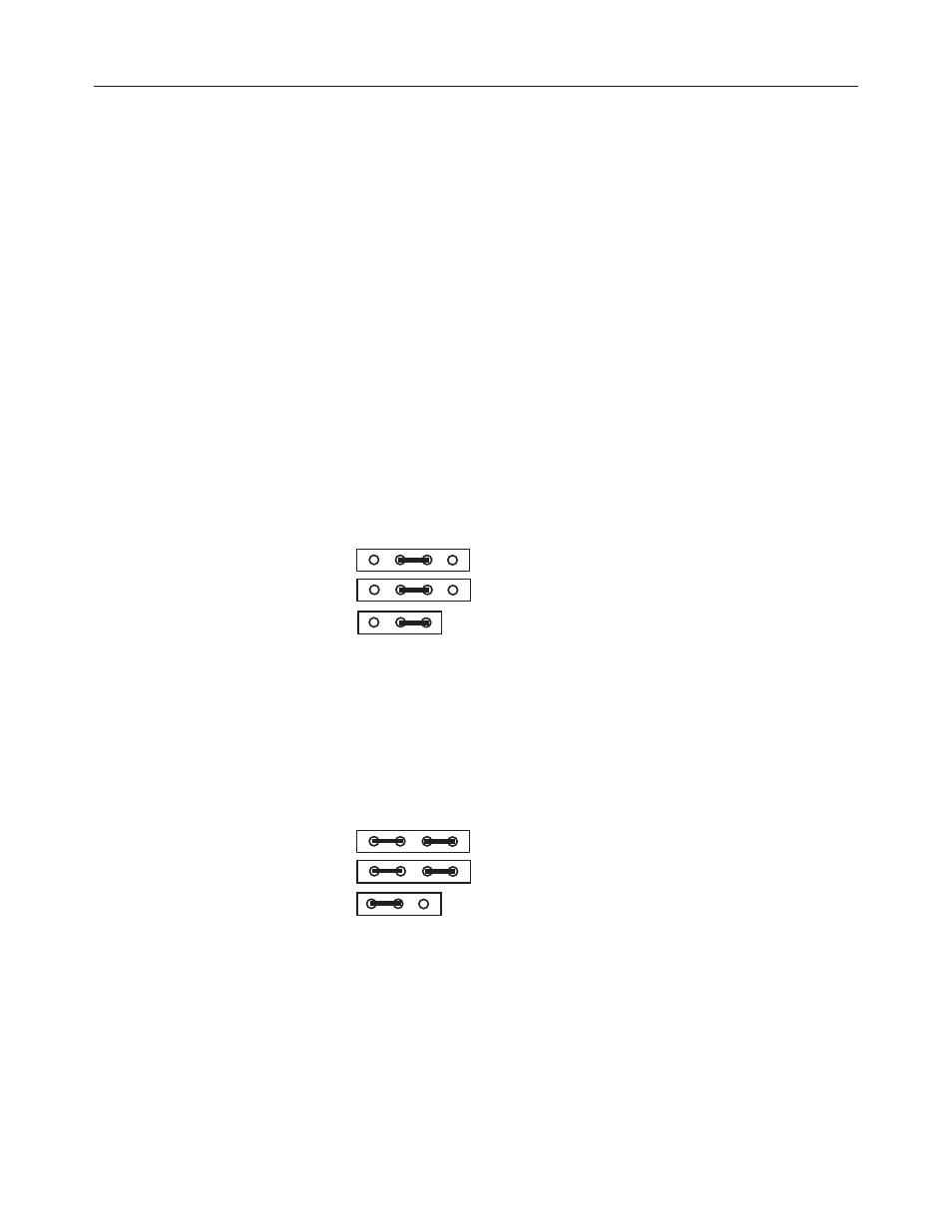
Setting For RTD or
Resistance Inputs
The module will either support zero RTD or resistance inputs or four
RTD or resistance inputs in channels 4 through 7. To properly
configure JP9 and JP10 for RTD or resistance, set the shunts across
pins 2 and 3 of the four pin headers. JP12 also needs to have pins 2
and 3 connected when RTD or resistance are to be used, as shown
below.
JP9
JP10
JP12
Setting For Non-RTD
or Resistance Inputs
If RTD and resistance inputs are not used, and channels 4 through 7
are to be defined as thermocouple inputs, current inputs, millivolt or
voltage inputs, jumper pins 1 and 2 together, jumper pins 3 and 4
together, of JP9 and JP10, as defined below. JP12 also needs to have
pins 1 and 2 connected when RTD and resistance inputs are not in
use.
JP9
JP10
JP12