Table 3-14, Spi interface pin signals (j19), Table 3-15 – ADLINK CoreModule 435 User Manual
Page 38: Lpc interface pin signals (j20), Serial peripheral interface (spi), Low pin count interface (lpc)
Chapter 3
Hardware
32
Reference Manual
CoreModule 435
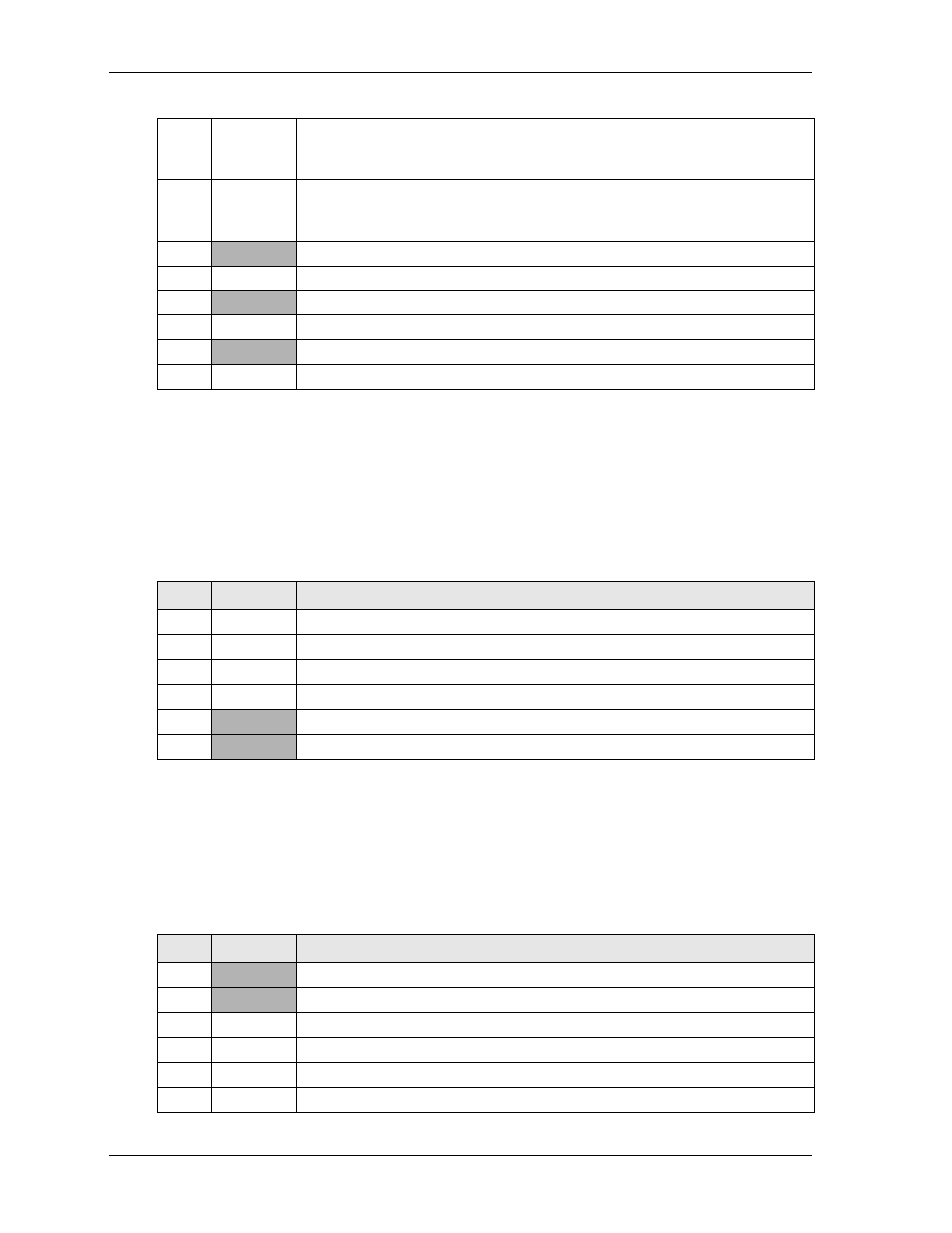
Note: The shaded table cells denote power or ground.
Serial Peripheral Interface (SPI)
The CoreModule 435 provides a 16Mbit SPI Flash controller (U6) for data storage. An SPI header (J19)
provides user access to the SPI Flash controller through an external SPI Bus.
describes the pin signals of the SPI interface, which uses a single-row, 6-pin header with 0.100"
(2.54mm) pitch.
Note: The shaded table cells denote power or ground.
Low Pin Count Interface (LPC)
The LPC interface provides expansion for custom LPC devices.
describes the pin signals of the LPC interface, which uses a 10-pin female header with 2 rows,
odd/even sequence (1, 2), and 0.050" (1.27mm) pitch.
37
HSYNC
Horizontal Sync – This signal is used for the digital horizontal sync output to the
CRT. Also used (with VSYNC) to signal power management state information to
the CRT per the VESA
™ DPMS™ standard.
38
VSYNC
Vertical Sync – This signal is used for the digital vertical sync output to the CRT.
Also used (with HSYNC) to signal power management state information to the
CRT per the VESA
™ DPMS™ standard.
39
AGNDR
Analog Ground for Red
40
RED
Red – This pin provides the Red analog output to the CRT.
41
AGNDG
Analog Ground for Green
42
GREEN
Green – This pin provides the Green analog output to the CRT.
43
AGNDB
Analog Ground for Blue
44
BLUE
Blue – This pin provides the Blue analog output to the CRT.
Table 3-14. SPI Interface Pin Signals (J19)
Pin #
Signal
Description
1
EXT_CS
SPI Chip Select
2
EXT_CLK
SPI Clock
3
EXT_DO
SPI Data Out
4
EXT_DI
SPI Data In
5
V.3.3
+3.3 Volts Power
6
GND
Ground
Table 3-15. LPC Interface Pin Signals (J20)
Pin #
Signal
Description
1
V.3.3
+3.3 Volts Power
2
GND
Ground
3
DRQ
DMA Request
4
AD3
Command, Address, and Data 3
5
SERIRQ
Serial Interrupt Request
6
AD2
Command, Address, and Data 2
Table 3-13. Video Interface Pin Signals (J11) (Continued)