ADLINK ETX-PVR User Manual
Page 35
Chapter 3
Hardware
ETX-PVR
Reference Manual
29
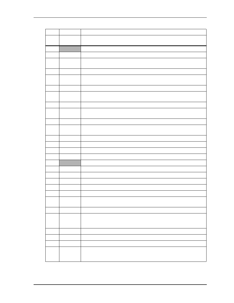
49
SA5
System Address 5 – Refer to SA0, pin-39 for more information.
50
IRQ4
Interrupt Request 4 – Asserted by a device when it has pending interrupt
request. Only one device may use the request line at a time.
51, 52
VCC
DC Power – +5 volts +/- 5%
53
SA6
System Address 6 – Refer to SA0, pin-39 for more information.
54
IRQ5
Interrupt Request 5 – Asserted by a device when it has pending interrupt
request. Only one device may use the request line at a time.
55
SA7
System Address 7 – Refer to SA0, pin-39 for more information.
56
IRQ6
Interrupt Request 6 – Asserted by a device when it has pending interrupt
request. Only one device may use the request line at a time.
57
SA8
System Address 8 – Refer to SA0, pin-39 for more information.
58
IRQ7
Interrupt Request 7 – Asserted by a device when it has pending interrupt
request. Only one device may use the request line at a time.
59
SA9
System Address 9 – Refer to SA0, pin-39 for more information.
60
SYSCLK
System Clock – This is a free running clock typically in the 8 MHz to 10 MHz
range, although its exact frequency is not guaranteed.
61
SA10
System Address 10 – Refer to SA0, pin-39 for more information.
62
REFSH*
Memory Refresh – This signal is driven low to indicate a memory refresh cycle
is in progress. Memory is refreshed every 15.6 usec.
63
SA11
System Address 11 – Refer to SA0, pin-39 for more information.
64 NS
Not
Supported
65
SA12
System Address 12 – Refer to SA0, pin-39 for more information.
66 NS
Not
Supported
67, 68
GND
Ground
69
SA13
System Address 13 – Refer to SA0, pin-39 for more information.
70 NS
Not
Supported
71
SA14
System Address 14 – Refer to SA0, pin-39 for more information.
72 NS
Not
Supported
73
SA15
System Address 15 – Refer to SA0, pin-39 for more information.
74
IOR*
I/O Read – This strobe signal is driven by the owner of the bus (ISA bus master)
and instructs the selected I/O device to drive read data onto the data bus.
75
SA16
System Address 16 – Refer to SA0, pin-39 for more information.
76
IOW*
I/O Write – This strobe signal is driven by the owner of the bus (ISA bus
master) and instructs the selected I/O device to capture the write data on the
data bus.
77
SA18
System Address 18 – Refer to SA0, pin-39 for more information.
78
SA17
System Address 17 – Refer to SA0, pin-39 for more information.
79
SA19
System Address 19 – Refer to SA0, pin-39 for more information.
80
SMEMR*
System Memory Read – This signal is used by bus owner to request a memory
device to drive data onto the data bus and only active for lower 1 MB. Used for
legacy compatibility with 8-bit cards.
Table 3-5. Complete X2 ISA Bus Interface Pin Signal Descriptions (J2) (Continued)