X2 isa bus interface (j2), Table 3-5 – ADLINK ETX-PVR User Manual
Page 33
Chapter 3
Hardware
ETX-PVR
Reference Manual
27
Note: The shaded areas denote power or ground. The * symbol indicates the signal is Active Low.
X2 ISA Bus Interface (J2)
The J2, 100-pin connector is used for standard ISA interface connections. The CPU does not directly support
an ISA expansion interface. A provision for ISA bus capabilities is provided in this connector through an on-
board PCI-to-ISA bridge. Refer to
for pin definitions of the X2 interface.
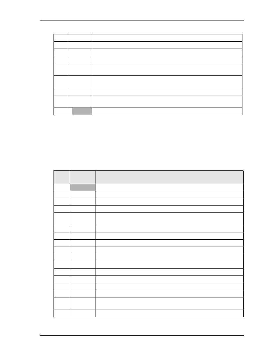
91
AD30
Address/Data bus 30 – Refer to J1, pin-23 for more information.
92
USB1+
Universal Serial Bus Port 1 Data Positive Polarity
93
PCIRST*
PCI Bus Reset – Signal resets entire PCI Bus. Asserted during a system reset.
94
AD31
Address/Data bus 31 – Refer to J1, pin-23 for more information.
95
INTC*
Interrupt C – This signal is used to request an interrupt and only has meaning on
a multi-function device.
96
INTD*
Interrupt D – This signal is used to request an interrupt and only has meaning on
a multi-function device.
97
INTA*
Interrupt A – This signal is used to request an interrupt.
98
INTB*
Interrupt B – This signal is used to request an interrupt and only has meaning on
a multi-function device.
99, 100 GND
Ground
Table 3-5. Complete X2 ISA Bus Interface Pin Signal Descriptions (J2)
J2
Pin #
Signal
Description
1, 2
GND
Ground
3
SD14
System Data 14 – These signals (0 to 19) provide system data bits.
4
SD15
System Data 15 – Refer to SD14, pin-3 for more information.
5
SD13
System Data 13 – Refer to SD14, pin-3 for more information.
6
MASTER* Bus Master – This signal is used by an ISA board to gain ownership of the ISA
bus.
7
SD12
System Data 12 – Refer to SD14, pin-3 for more information.
8 NS
Not
Supported
9
SD11
System Data 11 – Refer to SD14, pin-3 for more information.
10 NS
Not
Supported
11
SD10
System Data 10 – Refer to SD14, pin-3 for more information.
12 NS
Not
Supported
13
SD9
System Data 9 – Refer to SD14, pin-3 for more information.
14 NS
Not
Supported
15
SD8
System Data 8 – Refer to SD14, pin-3 for more information.
16 NS
Not
Supported
17
MEMW*
Memory Write – This signal instructs a selected memory device to store data
currently on the data bus. It is active on all memory write cycles.
18 NS
Not
Supported
Table 3-4. Complete X1 Interface Pin Signal Descriptions (J1) (Continued)