Audio interface, Table 3-4, Complete x1 interface pin signal descriptions (j1) – ADLINK ETX-PVR User Manual
Page 30
Chapter 3
Hardware
24
Reference Manual
ETX-PVR
Audio Interface
The Realtek HD Audio CODEC (ALC262) on the ETX-PVR supports the HDA Link protocol and the
supported features in the following list.
•
Supports audio amplifier on baseboard
•
PC-Beep pass through to Line Out while reset is held Active Low
•
True Line Level Output with volume control independent of Line Out
•
Digital 3V and 5V compliant
provides a complete list of the ETX J1 connector signals.
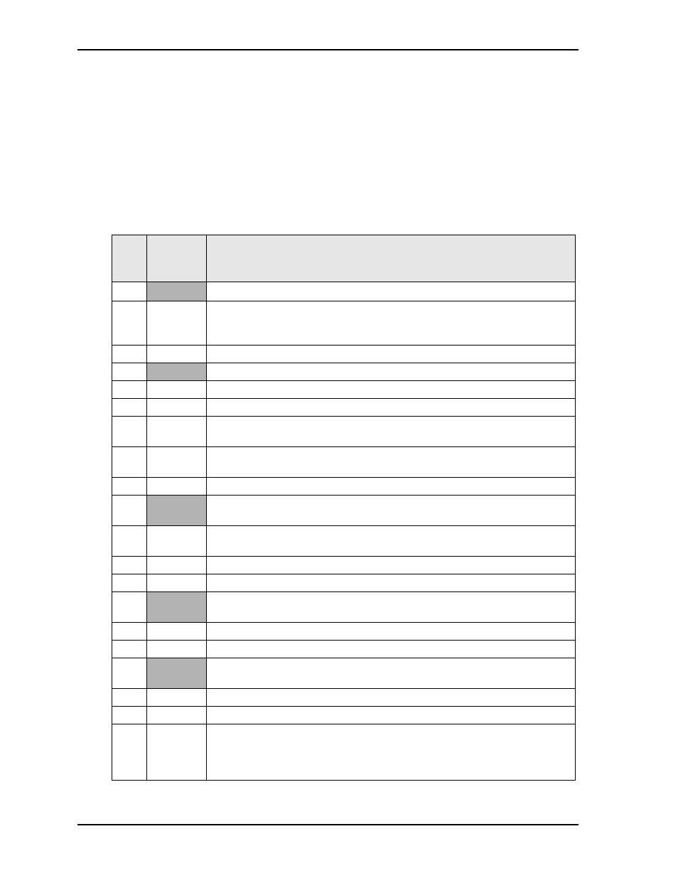
Table 3-4. Complete X1 Interface Pin Signal Descriptions (J1)
J1
Pin
#
Signal
Description
1, 2
GND
Ground
3
PCICLK3
PCI clock 3 – This signal line is one of four signal lines. These clock signals
provide the timing outputs for four external PCI devices and the timing for all
transactions on the PCI bus.
4
PCICLK4
PCI clock 4 – Refer to J1, pin-3 for more information.
5, 6
GND
Ground
7
PCICLK1
PCI clock 1 – Refer to J1, pin-3 for more information.
8
PCICLK2
PCI clock 2 – Refer to J1, pin-3 for more information.
9
REQ3*
Bus Request 3 – This signal line is one of four signal lines. These signals indicate
to the arbiter that the device desires use of the bus.
10
GNT3*
Grant 3 – This signal line is one of four signal lines. These signal lines indicate
access has been granted to the requesting device (PCI Masters).
11
GNT2*
Grant 2 – Refer to J1, pin-10 for more information.
12
+3.3V
+3.3 volts +/- 5% (Caution: This signal is generated by the ETX-PVR.)
[Note: This signal is not supported on ETX-PVR-R-14, R-16, and R-18 models.]
13
REQ2*
Bus Request 2 – This signal line is one of four signal lines. These signals indicate
the device desires use of the bus to the arbiter.
14
GNT1*
Grant 1 – Refer to J1, pin-10 for more information.
15
REQ1*
Bus Request 1 – Refer to J1, pin-13 for more information.
16
+3.3V
+3.3 volts +/- 5% (Caution: This signal is generated by the ETX-PVR.)
[Note: This signal is not supported on ETX-PVR-R-14, R-16, and R-18 models.]
17
GNT0*
Grant 0 – Refer to J1, pin-10 for more information.
18 NC
Not
Connected
(Reserved)
19,
20
VCC
DC Power – +5 volts +/- 5%
21
SERIRQ
Serial Interrupt Request – This signal supports the serial interrupt protocol.
22
REQ0*
Bus Request 0 – Refer to J1, pin-13 for more information.
23
AD0
Address/Data bus 0 – These signals
PCI connector pins. During the address phase of a PCI cycle, AD31–AD0
contain a 32-bit address or other destination information. During the data phase,
AD31 – AD0 contain data.