ADLINK ETX-PVR User Manual
Page 31
Chapter 3
Hardware
ETX-PVR
Reference Manual
25
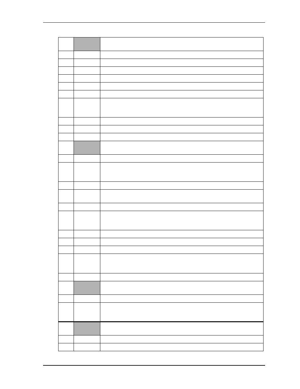
24
+3.3V
+3.3 volts +/- 5% (Caution: This signal is generated by the ETX-PVR.)
[Note: This signal is not supported on ETX-PVR-R-14, R-16, and R-18 models.]
25
AD1
Address/Data bus 1 – Refer to J1, pin-23 for more information.
26
AD2
Address/Data bus 2 – Refer to J1, pin-23 for more information.
27
AD4
Address/Data bus 4 – Refer to J1, pin-23 for more information.
28
AD3
Address/Data bus 3 – Refer to J1, pin-23 for more information.
29
AD6
Address/Data bus 6 – Refer to J1, pin-23 for more information.
30
AD5
Address/Data bus 5 – Refer to J1, pin-23 for more information.
31
CBE0*
PCI Bus Command/Byte Enable 0 – This signal line is one of four signal lines
multiplexed on the same pins, so that during the address cycle, the command is
defined and during the data cycle, the byte enable is defined.
32
AD7
Address/Data bus 7 – Refer to J1, pin-23 for more information.
33
AD8
Address/Data bus 8 – Refer to J1, pin-23 for more information.
34
AD9
Address/Data bus 9 – Refer to J1, pin-23 for more information.
35,
36
GND
Ground
37
AD10
Address/Data bus 10 – Refer to J1, pin-23 for more information.
38
AUXAL
Auxiliary A Input Left – This signal is normally used for an external CD-ROM
analog output or similar live-level audio source. Minimum input impedance is 5k
Ohms and nominal input level is 1 volt RMS.
39
AD11
Address/Data bus 11 – Refer to J1, pin-23 for more information.
40
MIC
Microphone reference signal – This microphone input signal has a minimum
input impedance of 5k Ohms, and the maximum input voltage is 0.15 V p-p.
41
AD12
Address/Data bus 12 – Refer to J1, pin-23 for more information.
42
AUXAR
Auxiliary A Input Right – This signal is normally used for an external CD-ROM
analog output or similar live-level audio source. Minimum input impedance is 5k
Ohms and nominal input level is 1 volt RMS.
43
AD13
Address/Data bus 13 – Refer to J1, pin-23 for more information.
44 NC
Not
Connected
45
AD14
Address/Data bus 14 – Refer to J1, pin-23 for more information.
46
SNDL
Stereo Line Output Left channel – Output signal has a nominal 1 volt RMS level
into 10k impedance load. This output signal can not drive low-impedance
speakers directly.
47
AD15
Address/Data bus 15 – Refer to J1, pin-23 for more information.
48
ASGND
Analog Ground – This ground is used for the sound controller and an external
amplifier to achieved the lowest audio noise levels.
49
CBE1*
Bus Command and Byte Enable 1 – Refer to J1, pin-31 for more information.
50
SNDR
Stereo Line Output Right channel – This output signal has a nominal level of 1
volt RMS into 10k impedance load. This output signal can not drive low-
impedance speakers directly
51,
52
VCC
DC Power – +5 volts +/- 5%
53
PAR
PCI bus Parity bit – This signal is even parity bit on AD[31:0] and CBE[3:0]*.
54
SERR*
System Error – This signal is for reporting address parity errors.
Table 3-4. Complete X1 Interface Pin Signal Descriptions (J1) (Continued)