ADLINK ETX-PVR User Manual
Page 34
Chapter 3
Hardware
28
Reference Manual
ETX-PVR
19
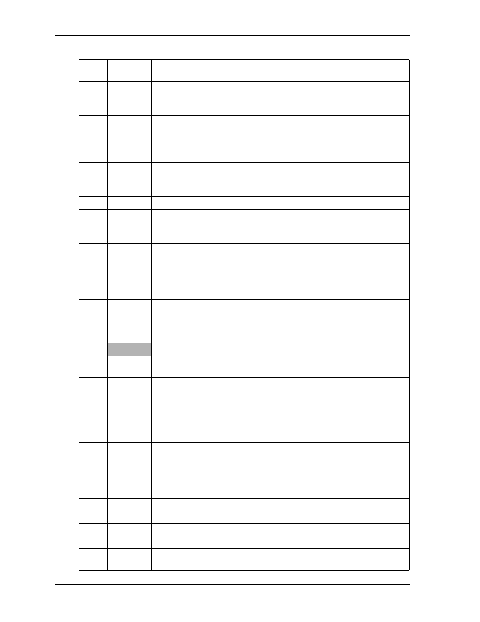
MEMR*
Memory Read – This signal instructs a selected memory device to drive data
onto the data bus. It is active on all memory read cycles.
20 NS
Not
Supported
21
LA17
Latchable Address 17 – These signals (0-23) must be latched by the resource if
the line is required for the entire data cycle.
22 NS
Not
Supported
23
LA18
Latchable Address 18 – Refer to LA17, pin-21 for more information.
24
IRQ14
Interrupt Request 14 – Asserted by a device when it has pending interrupt
request. Only one device may use the request line at a time.
25
LA19
Latchable Address 19 – Refer to LA17, pin-21 for more information.
26
IRQ15
Interrupt Request 15 – Asserted by a device when it has pending interrupt
request. Only one device may use the request line at a time.
27
LA20
Latchable Address 20 – Refer to LA17, pin-21 for more information.
28
IRQ12
Interrupt Request 12 – Asserted by a device when it has pending interrupt
request. Only one device may use the request line at a time.
29
LA21
Latchable Address 21– Refer to LA17, pin-21 for more information.
30
IRQ11
Interrupt Request 11 – Asserted by a device when it has pending interrupt
request. Only one device may use the request line at a time.
31
LA22
Latchable Address 22 – Refer to LA17, pin-21 for more information.
32
IRQ10
Interrupt Request 10 – Asserted by a device when it has pending interrupt
request. Only one device may use the request line at a time.
33
LA23
Latchable Address 23 – Refer to LA17, pin-21 for more information.
34
IO16*
I/O Chip Select 16 – This signal is driven low by an I/O slave device to indicate
it is capable of performing a 16-bit I/O data transfer. This signal is driven from
a decode of the SA15 to SA0 address lines.
35, 36
GND
Ground
37
SBHE*
System Byte High Enable – This signal is driven low to indicate a transfer of
data on the high half of the data bus (D15 to D8).
38
M16*
Memory Chip Select 16 – This signal is driven low by a memory slave device to
indicates it is cable of performing a 16-bit memory data transfer. This signal is
driven from a decode of the LA23 to LA17 address lines.
39
SA0
System Address 0 – These signals (0 to 19) provide system address bits.
40
OSC
Oscillator – This clock signal operates at 14.3 MHz. This signal is not
synchronous with the system clock (SYSCLK).
41
SA1
System Address 1– Refer to SA0, pin-39 for more information.
42
BALE
Buffered Address Latch Enable – This signal is used to latch the LA23 to LA17
signals or decodes of these signals. Addresses are latched on the falling edge of
BALE.
43
SA2
System Address 2 – Refer to SA0, pin-39 for more information.
44 NS
Not
Supported
45
SA3
System Address 3 – Refer to SA0, pin-39 for more information.
46 NS
Not
Supported
47
SA4
System Address 4 – Refer to SA0, pin-39 for more information.
48
IRQ3
Interrupt Request 3 – Asserted by a device when it has pending interrupt
request. Only one device may use the request line at a time.
Table 3-5. Complete X2 ISA Bus Interface Pin Signal Descriptions (J2) (Continued)