B1 connector pinout – Digilent 410-044-10P-KIT User Manual
Page 51
Spartan-3 Starter Kit Board User Guide
51
UG130 (v1.1) May 13, 2005
1-800-255-7778
Expansion Connectors
R
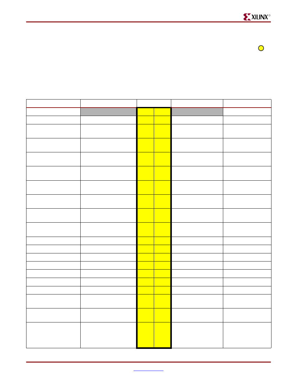
B1 Connector Pinout
The B1 expansion connector is located on the right edge of the board, as indicated by
in
Table 13-4
provides the pinout for the B1 connector. The FPGA connections are
specified in parentheses.
Most of the B1 expansion connector pins connect only with the FPGA and are not shared.
Pins 36 through 40 include the signals required to configure the FPGA in Master or Slave
Serial mode. These same pins plus pins 5, 7, 9, 11, 13, 15, 17, 19, and 20 provide the signals
required to configure the FPGA in Master or Slave Parallel mode.
19
Table 13-4:
Pinout for B1 Expansion Connector
Schematic Name
FPGA Pin
Connector
FPGA Pin
Schematic Name
GND
1
2
VU (+5V)
V
CCO
(+3.3V)
V
CCO
(all banks)
3
4
(C10)
PB-ADR0
PB-DB0
(T3)
FPGA RD_WR_B config
5
6
(E10)
PB-ADR1
PB-DB1
(N11)
FPGA D1 config
7
8
(C11)
PB-ADR2
PB-DB2
(P10)
FPGA D2 config
9
10
(D11)
PB-ADR3
PB-DB3
(R10)
FPGA D3 config
11
12
(C12)
PB-ADR4
PB-DB4
(T7)
FPGA D4 config
13
14
(D12)
PB-ADR5
PB-DB5
(R7)
FPGA D5 config
15
16
(E11)
PB-WE
PB-DB6
(N6)
FPGA D6 config
17
18
(B16)
PB-OE
PB-DB7
(M6)
FPGA D7 config
19
20
(R3)
FPGA CS_B config
PB-CS
PB-CLK
(C15)
21
22
(C16)
MB1-DB0
MB1-DB1
(D15)
23
24
(D16)
MB1-DB2
MB1-DB3
(E15)
25
26
(E16)
MB1-DB4
MB1-DB5
(F15)
27
28
(G15)
MB1-DB6
MB1-DB7
(G16)
29
30
(H15)
MB1-ASTB
MB1-DSTB
(H16)
31
32
(J16)
MB1-WRITE
MB1-WAIT
(K16)
33
34
(K15)
MB1-RESET
MB1-INT
(L15)
35
36
(B3)
FPGA PROG_B
PROG-B
DONE
(R14)
FPGA DONE
37
38
(N9)
FPGA INIT_B
INIT
CCLK
(T15)
FPGA CCLK
Connects to (A14) via
390
Ω resistor
39
40
(M11)
DIN