Flash read” option – Digilent 410-044-10P-KIT User Manual
Page 39
Spartan-3 Starter Kit Board User Guide
39
UG130 (v1.1) May 13, 2005
1-800-255-7778
“Flash Read” Option
R
“Flash Read” Option
The Spartan-3 Starter Kit Board includes a 2Mbit Platform Flash configuration PROM. The
XC3S200 FPGA on the board only requires slightly less than 1Mbit for configuration data.
The remainder of the Platform Flash is available to store other non-volatile data, such as
revision codes, serial numbers, coefficients, an Ethernet MAC ID, or code for an embedded
processor, such as MicroBlaze, within the FPGA.
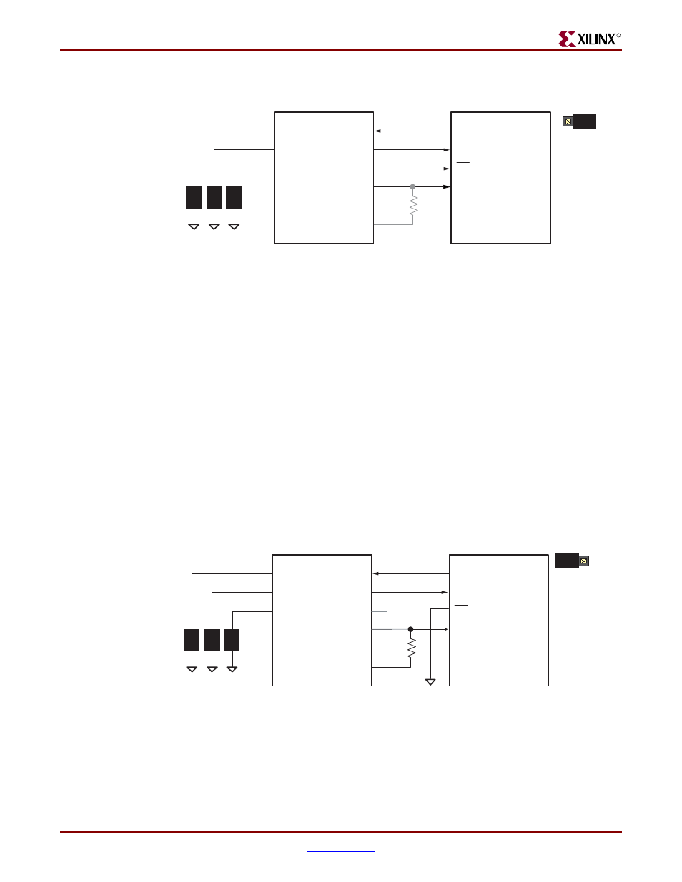
To allow the FPGA to read from Platform Flash after configuration, the JP1 jumper must be
properly positioned, as shown in
Figure 10-2
. When the jumper is in this position, the
Platform Flash is always enabled. After FPGA configuration completes, the FPGA
application drives the INIT_B pin High, FPGA pin N9. Consequently, the Platform Flash
data pointer is not reset and points to the additional data following the FPGA
configuration data. To read any subsequent data, the FPGA application generates
additional clock pulses on the RCLK signal from FPGA pin A14. After configuration, the
FPGA’s CCLK output is three-stated with a pull-up resistor to V
CCAUX
(2.5V). The
Platform Flash presents serial data on the FPGA’s DIN pin, pin M11.
The resistor between the CCLK output and FPGA pin A14 prevents any accidental
conflicts between the two signals.
Figure 10-1:
Default Platform Flash Option
CCLK
INIT_B
USER I/O
DONE
CLK
D0
OE/RESET
CE
DIN/D0
M0
M1
M2
Spartan-3 FPGA
Platform Flash
J8
MODE
JP1
Default
RCLK
UG130_c10_01_060704
Figure 10-2:
Read Additional Data from Platform Flash by Setting the JP1 Jumper
CCLK
INIT_B
USER I/O
DONE
CLK
D0
OE/RESET
CE
DIN/D0
M0
M1
M2
Spartan-3 FPGA
Platform Flash
J8
MODE
RCLK
UG130_c10_02_060404
Flash Read
JP1
(M11)
(N9)
(A14)
(xx) = FPGA pin number