Write enable and output enable control signals, Sram data signals, chip enables, and byte enables – Digilent 410-044-10P-KIT User Manual
Page 13
Spartan-3 Starter Kit Board User Guide
13
UG130 (v1.1) May 13, 2005
1-800-255-7778
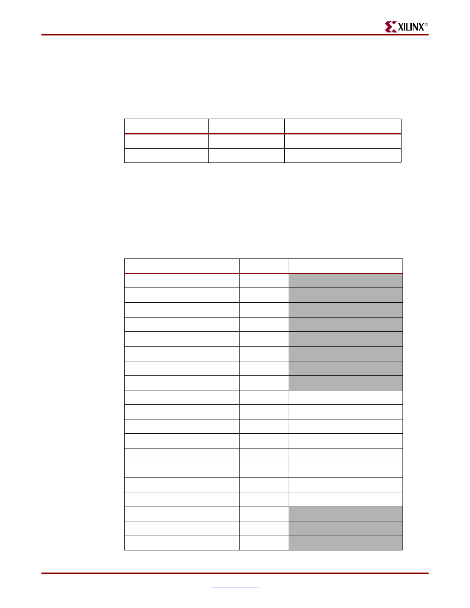
Write Enable and Output Enable Control Signals
R
Write Enable and Output Enable Control Signals
Both 256Kx16 SRAMs share common output enable (OE#) and write enable (WE#) control
lines, as shown in
Table 2-2
. These control signals also connect to the A1 Expansion
Connector (refer to
“Expansion Connectors,” page 47
SRAM Data Signals, Chip Enables, and Byte Enables
The data signals, chip enables, and byte enables are dedicated connections between the
FPGA and SRAM.
Table 2-3
shows the FPGA pin connections to the SRAM designated
IC10 in
.
Table 2-4
shows the FPGA pin connections to SRAM IC11. To disable an
SRAM, drive the associated chip enable pin High.
Table 2-2:
External SRAM Control Signal Connections to Spartan-3 FPGA
Signal
FPGA Pin
A1 Expansion Connector Pin
OE#
K4
16
WE#
G3
18
Table 2-3:
SRAM IC10 Connections
Signal
FPGA Pin
A1 Expansion Connector Pin
IO15
R1
IO14
P1
IO13
L2
IO12
J2
IO11
H1
IO10
F2
IO9
P8
IO8
D3
IO7
B1
19
IO6
C1
17
IO5
C2
15
IO4
R5
13
IO3
T5
11
IO2
R6
9
IO1
T8
7
IO0
N7
5
CE1 (chip enable IC10)
P7
UB1 (upper byte enable IC10)
T4
LB1 (lower byte enable IC10)
P6