A2 connector pinout – Digilent 410-044-10P-KIT User Manual
Page 50
50
Spartan-3 Starter Kit Board User Guide
1-800-255-7778
UG130 (v1.1) May 13, 2005
Chapter 13: Expansion Connectors and Boards
R
The A1 expansion connector shares connections with the 256Kx16 SRAM devices,
specifically the SRAM address lines, the OE# and WE# control signals, and the eight least-
significant data lines to SRAM IC10 only. Similarly, the JTAG chain is available on pins 36
through 40. Pin 20 is the FPGA DOUT/BUSY configuration signal and toggles during the
FPGA configuration process.
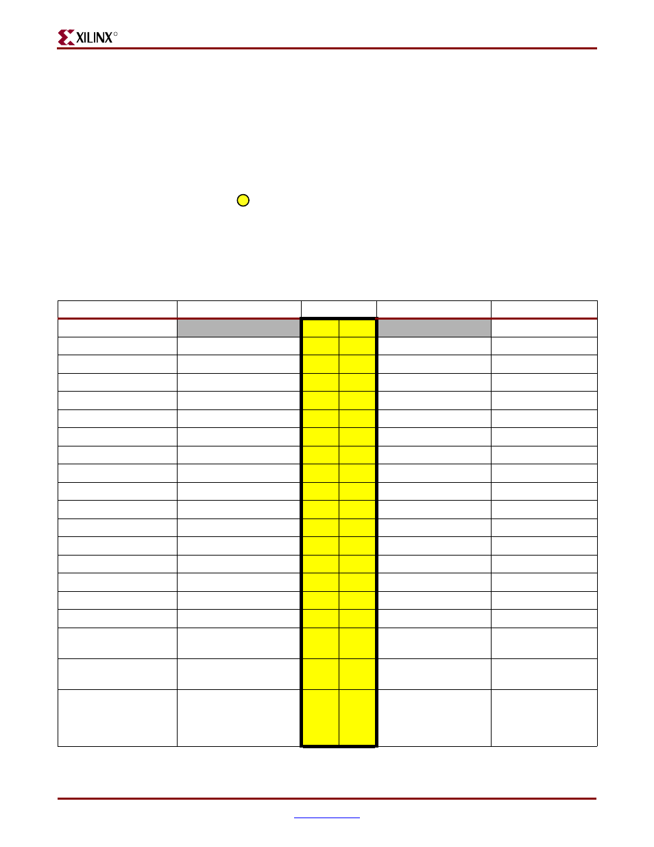
A2 Connector Pinout
The A2 expansion connector is located along the top edge of the board, on the right, as
indicated by
in
Figure 13-3
provides the pinout for the A2 connector. The
FPGA connections are specified in parentheses.
Most of the A2 expansion connector pins connect only with the FPGA and are not shared.
Pin 35 connects to the auxiliary clock socket, if an oscillator is installed in the socket. Pins
36 through 40 include the signals required to configure the FPGA in Master or Slave Serial
mode.
20
Table 13-3:
Pinout for A2 Expansion Connector
Schematic Name
FPGA Pin
Connector
FPGA Pin
Schematic Name
GND
1
2
VU (+5V)
V
CCO
(+3.3V)
V
CCO
(all banks)
3
4
(E6)
PA-IO1
PA-IO2
(D5)
5
6
(C5)
PA-IO3
PA-IO4
(D6)
7
8
(C6)
PA-IO5
PA-IO6
(E7)
9
10
(C7)
PA-IO7
PA-IO8
(D7)
11
12
(C8)
PA-IO9
PA-IO10
(D8)
13
14
(C9)
PA-IO11
PA-IO12
(D10)
15
16
(A3)
PA-IO13
PA-IO14
(B4)
17
18
(A4)
PA-IO15
PA-IO16
(B5)
19
20
(A5)
PA-IO17
PA-IO18
(B6)
21
22
(B7)
MA2-DB0
MA2-DB1
(A7)
23
24
(B8)
MA2-DB2
MA2-DB3
(A8)
25
26
(A9)
MA2-DB4
MA2-DB5
(B10)
27
28
(A10)
MA2-DB6
MA2-DB7
(B11)
29
30
(B12)
MA2-ASTB
MA2-DSTB
(A12)
31
32
(B13)
MA2-WRITE
MA2-WAIT
(A13)
33
34
(B14)
MA2-RESET
MA2-INT/GCK4
(D9)
Oscillator socket
35
36
(B3)
FPGA PROG_B
PROG-B
DONE
(R14)
FPGA DONE
37
38
(N9)
FPGA INIT_B
INIT
CCLK
(T15)
FPGA CCLK
Connects to (A14) via
390
Ω resistor
39
40
(M11)
DIN