Digilent DIO2 User Manual
Page 8
Digilab DIO2 Reference Manual
Digilent, Inc.
www.digilentinc.com
page 8 of 19
Copyright Digilent, Inc. All rights reserved. Other product and company names mentioned may be trademarks of their respective owners.
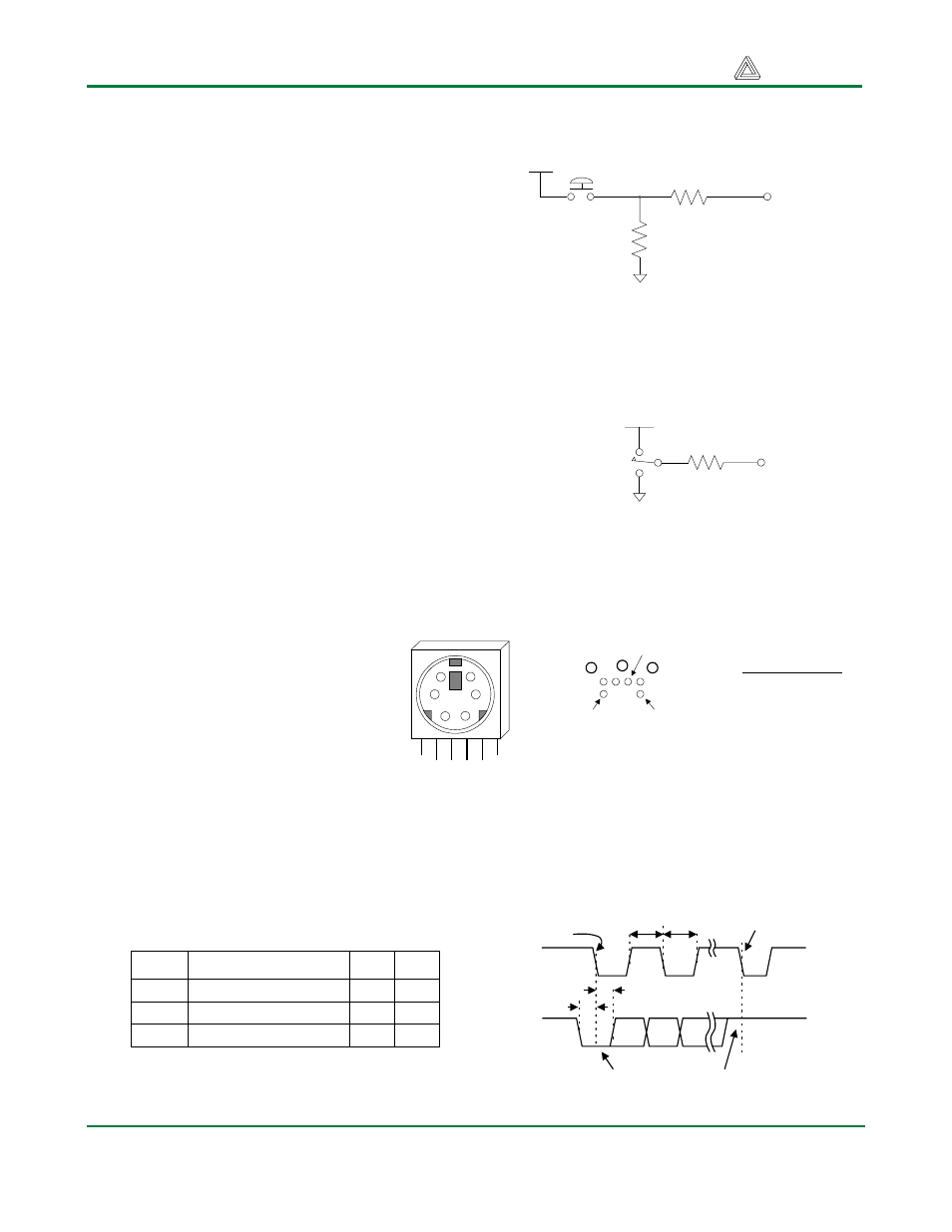
Pushbuttons
Outputs from the 15 momentary-contact push buttons
are normally low, and are driven high only while the
button is actively pressed. The buttons exhibit a worst-
case bounce time of about 1ms. A 4.7K series resistor
provides some debounce filtering and ESD protection.
When configured with the code shown in the
appendix, the CPLD on the DIO2 board makes all
button signals available on the bus in two successive
readable address locations (0 and 1).
Switches
The eight slide switches can be used to connect either Vdd or
GND to eight pins on the CPLD. The switches exhibit about 2ms
of bounce, and no active debouncing circuit is employed. A 4.7K-
ohm series resistor is used for nominal input protection. When
configured with the code shown in the appendix, the CPLD on the
DIO2 board makes all switch signals available on the bus at
address location 2.
PS2 port
The DIO2 board includes a 6-pin
mini-DIN connector that can
accommodate a PS2 mouse or PS2
keyboard connection. Both the
mouse and keyboard use a two-
wire serial bus (including clock
and data) to communicate with a
host device, and both drive the bus
with identical signal timings. Both
use 11-bit words that include a start, stop and odd parity bit, but the data packets are organized
differently, and the keyboard interface allows bi-directional data transfers (so the host device can
illuminate state LEDs on the keyboard).
PS2 Connector front view
Pin 1
Pin 5
Pin 6
Bottom-up
hole pattern
PS2 Pin Definitions
Pin Function
1 Data
2 Reserved
3 GND
4 Vdd
5 Clock
6 Reserved
1
5
3
2
4
6
Vdd
GND
RP10,12,14,16
4.7KOhm
RP8&9
4.7KOhm
To CPLD
GND
Vdd
To CPLD
RP6 & 7
4.7 KOhm
T
CK
T
SU
Edge 0
Edge 10
CLK
DATA
T
CK
T
SU
Clock time
Data-to-clock setup time
30us
5us
50us
25us
Symbol
Parameter
Min
Max
T
HLD
Clock-to-data hold time
5us
25us
T
HLD
T
CK
'1' stop bit
'0' start bit