Digilent DIO2 User Manual
Page 5
Digilab DIO2 Reference Manual
Digilent, Inc.
www.digilentinc.com
page 5 of 19
Copyright Digilent, Inc. All rights reserved. Other product and company names mentioned may be trademarks of their respective owners.
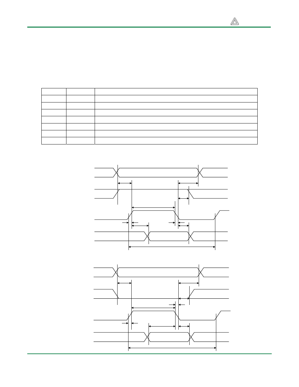
The display is connected to the DIO2 board by a 16-pin connector (pins 15 and 16 are for an optional
backlight, and they are not connected on the DIO2 board). The eight data bus signals and three strobes
are connected directly to the B connector on the DIO2 board (note the data lines are common with the
CPLD data bus), so the LCD can be controlled from a Digilab system board. Bus timings are shown
below. Note that the enable signal (E) serves as both output enable and write strobe (with an active
falling edge) depending on the state of the Read/Write (R/W) signal.
Pin No.
Symbol
Signal Description
1 Vss Signal
ground
2
Vdd
Power supply (5V)
3
Vo
Operating (contrast) voltage (LCD drive, typically 100mV at 20C)
4
RS
Register select: high for data transfer, low for instruction register
5
R/W
Read/write signal: high for read mode, low for write mode
6
E
Read/write strobe: high for read OE; falling edge writes data
7-14
Data Bus
Bi-directional data bus
LCD Read Cycle
tsu
th
th
tw
tr
tf
tD
tDH
tc
R/W
RS
E
DB0-DB7
LCD Write Cycle
tsu
th
th
tw
tr
tf
tsu1
th1
tc
R/W
RS
E
DB0-DB7