Digilent DIO2 User Manual
Page 14
Digilab DIO2 Reference Manual
Digilent, Inc.
www.digilentinc.com
page 14 of 19
Copyright Digilent, Inc. All rights reserved. Other product and company names mentioned may be trademarks of their respective owners.
between the onset of the HS pulse and the onset of the VS pulse is specified, so the designer can
arrange the counters to easily form video RAM addresses, or to minimize decoding logic for sync
pulse generation.
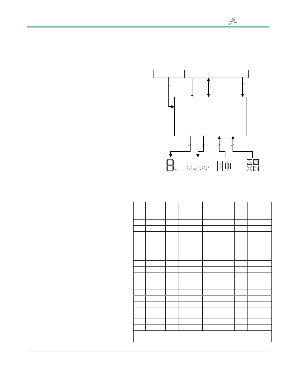
XC95108 CPLD
The block diagram shows the connections
between the CPLD and the devices on the DIO2
board. The CRT signals (HS, VS, and data), the
PS2 signals (clock and data), and the LCD
signals are routed directly from the B connector
to the devices, so they are not shown in the
diagram. The CPLD pin connections are shown
in the following table.
The CPLD is pre-configured with the circuit
specified by the attached VHDL code. This
circuit defines a communications bus between
the DIO2 board and the system board. Bus
signals and timings used by the CPLD interface
are shown below.
The CPLD device can be configured using the
Xilinx CAD tools and JTAG cable, or by using
the Digilab programmer board (the XC95 board
– see www.digitlentinc.com). To program the
board directly using a Xilinx JTAG cable,
a separate power supply must be used. The
supply can be attached either to the
VDD and GND pins on the test point
header, or to the legs of the LM2940
voltage regulator (pin1: 6-9VDC;
pin 2: GND). The JTAG signal wires
from the JTAG cable must be
attached to the JTAG signals
available on the A connector of the
DIO2 board, and the JTAG cable
power and GND signals must be
attached to the VDD and GND
signals on the test point header. To
program the board using the Digilent
programmer board, simply attach the
board, set switch 1 on the board to
EXT (for external device), and run
the Xilinx board configuration
software (refer to the XC95 board
documentation for more
information).
Pin Signal Pin Signal Pin Signal Pin Signal
1 D7
22 VCCIO
43 SW5
64 VCCIO
2 D6
23 AN2
44 SW7
65 BTNC
3 D5
24 AN3
45 SW6
66 BTN2
4 D4
25 AN4
46 SW8
67 LDA
5 D3
26 CC
47 BTN1 68 LDB
6 D2
27 GND
48 BTN5 69 LD9
7 D1
28 TDI
49
GND
70 LDC
8
GND
29
TMS
50 BTN6 71 LDD
9 WE
30 TCK
51 CD
72 LDE
10 CLK
31 CG
52 BTN3 73 VCCINT
11 D0
32 CF
53 BTN8 74 LDF
12 LD1
33 CB
54 BTNE 75 A5
13 CS
34 SW1
55 BTN4 76 OE
14 LD2
35 CA
56 BTNB 77 A4
15 LD3
36 CE
57 BTN7 78 VCCINT
16
GND
37 DP
58 BTN9 79 A3
17 LD4
38 VCCINT
59
TDO
80 A2
18 LD5
39 SW3
60 GND
81 A1
19 LD6
40 SW2
61 BTNA 82 LD0
20 LD7
41 SW4
62 BTND 83 A0
21 AN1
42 GND
63 LD8
84 BTN0
Table 5. CPLD pinout
Xilinx XC95108 CPLD
15 LEDs
4 displays
8 switches
15 button
keypad
Connector B
15
8
12
15
data
address &
control
Clk
9
8
Connector A
JTAG
4