Digilent DIO2 User Manual
Page 15
Digilab DIO2 Reference Manual
Digilent, Inc.
www.digilentinc.com
page 15 of 19
Copyright Digilent, Inc. All rights reserved. Other product and company names mentioned may be trademarks of their respective owners.
For further information on the Xilinx CPLD, please see the Xilinx data sheets available at the Xilinx
website (www.xilinx.com).
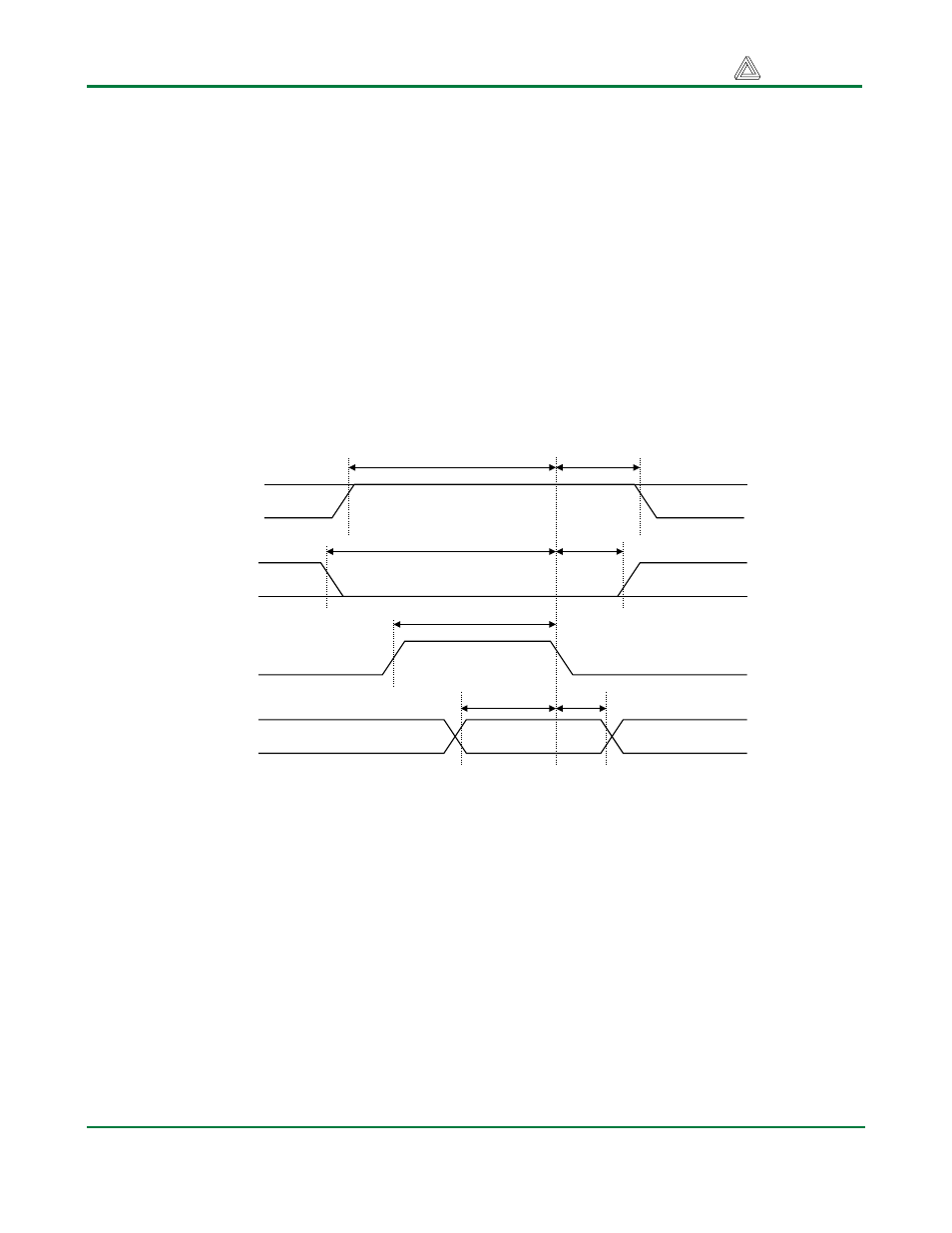
DIO2 bus timing information
The bi-directional data bus between the DIO2 board and an attached system board is used to write
LED and seven-segment display data, and to read the status of the slide switches and momentary push
buttons. The LED and seven-segment data is registered in the CPLD, but the switch and button data
simply passes through a multiplexor without being registered (if desired, registers can be added to the
CPLD configuration). Bus signals and timings are defined below for both write cycles and read cycles.
Note all strobes are active high. The WE signal drives a global clock line on the CPLD, and the OE
signal drives a global tri-state signal.
CPLD bus write cycle
CPLD bus read cycle
tw
th
OE
CS
WE
DB0-DB7
th
teoe
tsu
tdoe
tw