CANOGA PERKINS 2240 Fiber Optic Modem User Manual
Page 61
Chapter 4 Data Interfaces
Multi-Channel Interfaces
61
The previous V.35 interface Model MC2/435, did not conform to the ISO 2593 pinout and was the
predecessor to the MC2/436 interface. The MC2/436 went into production during mid-summer
1996. The signals listed in Table 4-13 have different pinouts on the MC2/435 versus the MC2/
436. The MC2/435 also did not support the Extra Clock for the receive data signal. This pinout
difference table is only included as a reference. MC2/436 interfaces can be identified by the
addition of a heatsink on the voltage regulator, VR1.
Calling Indicator (aka RI)
J
125
from modem
Local Loopback
L
141
to modem
Remote Loopback
N
140
to modem
Received Data (aka RXD)
R/T
104
from modem
Receiver Signal Element
V/X
115
from modem
Timing
DCE Source (aka SCR)
Transmitted Data (aka TXD)
P/S
103
to modem
Transmitter Signal Element
Y/AA
114
from modem
Timing
DCE Source (aka SCT)
Transmitter Signal Element
U/W
113
to modem
Timing
DTE Source (aka
SCTE)
Test Indicator (aka TM)
NN
142
from modem
Extra Clock for Receive Data
FF/DD *
–
to modem
* These pins carry signals which are not defined by V.35 or ISO 2593-1993. If a straight-
through cable is used, verify compatibility of this pin usage with the customer's
equipment.
NOTE 1: The 2240 connects the Shield pin to chassis ground.
NOTE 2: The extra clock signal is an enhancement added to -MC2 interfaces. MC2
interfaces with this capability can be identified by the addition of a heatsink on the
voltage regulator, VR1.
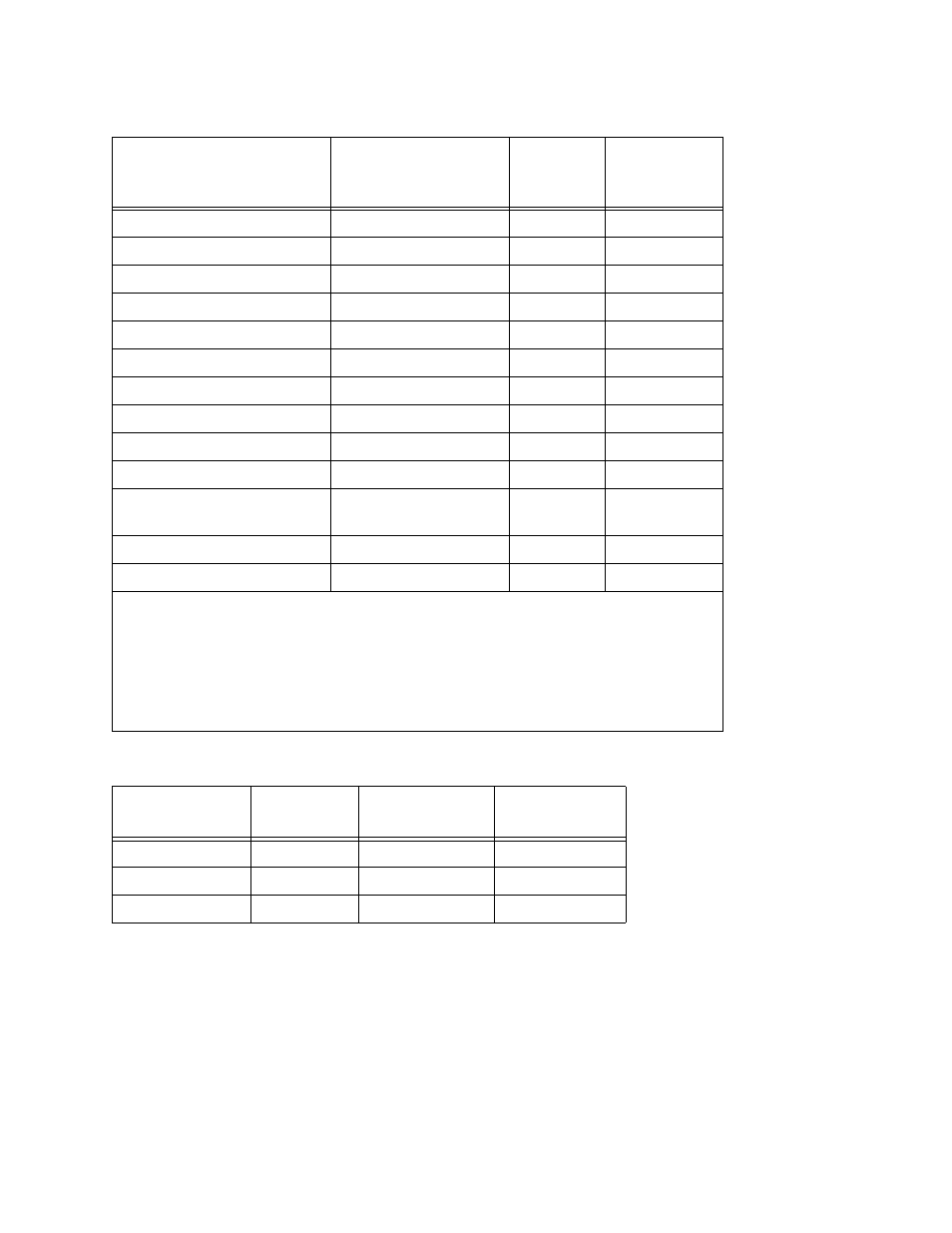
Table 4-13. Pinout Differences (MC2/435 vs. MC2/436)
Function
Pin (A/B)
CCITT Circuit
Number
Direction
Test Mode
C C
142
from modem
Local Loopback
E E
141
to modem
Remote Loopback D D
140
to modem
Table 4-12. CCITT V.35 Pinouts for MC2 (Continued)
Function
Pin (A/B)
CCITT
Circuit
Number
Direction