CANOGA PERKINS 2240 Fiber Optic Modem User Manual
Page 52
2240 Fiber Optic Modem User Manual
Chapter 4 Data Interfaces
CCITT V.35 (ISO 2593-1993) Model 436
52
NOTE: The previous V.35 interface, Model -435, did not conform to the ISO 2593
pinout and was the predecessor to the -436 interface. The signals listed in
Table 4-7 have different pinouts on the -435 versus the -436. The -435
also did not support the Extra Clock for the receive data signal. This pinout
difference table is only included as a reference.
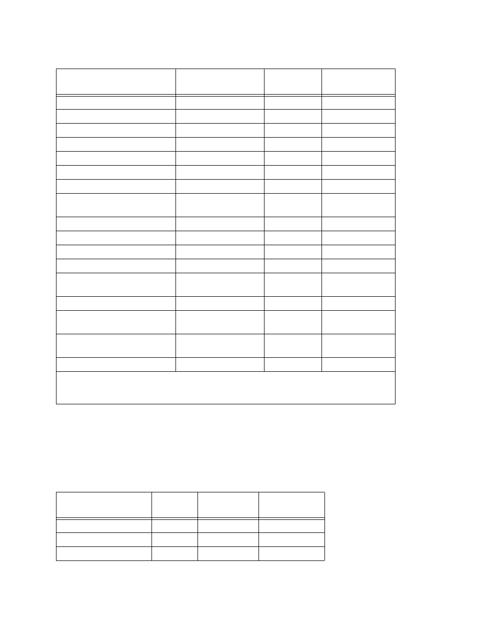
Signal Detector (aka DCD)
Data Terminal Ready (aka DTR)
H
108
to modem
Calling Indicator (aka RI)
J
125
from modem
Local Loopback
L
141
to modem
Remote Loopback
N
140
to modem
Received Data (aka RXD)
R/T
104
from modem
Receiver Signal Element
V/X
115
from modem
Timing
DCE Source (also
known as SCR)
Transmitted Data (aka TXD)
P/S
103
to modem
Transmitter Signal Element
Y/AA
114
from modem
Timing
DCE Source (aka SCT)
Transmitter Signal Element
U/W
113
to modem
Timing
DTE Source (aka
SCTE)
Test Indicator (aka TM)
NN
142
from modem
Secondary Transmit Data (aka
STD)
K*
-
to modem
Secondary Receive Data (aka
SRD)
M*
-
from modem
Extra Clock for Receive Data
FF/DD*
-
to modem
NOTE 1: The 2240 connects the Shield pin to chassis ground.
* These pins carry signals which are not defined by V.35 or ISO 2593-1993. If a straight-through
cable is used, verify compatibility of this pin usage with the customer's equipment.
Table 4-7. Pinout Differences (-435 vs. -436)
Function
Pin (A/B)
CCITT Circuit
Number
Direction
Test Indicator
C C
142
from modem
Secondary Receive Data
L
119
from modem
Local Loopback
E E
141
to modem
Table 4-6. CCITT V.35 Pinouts (Continued)
Function
Pin (A/B)
CCITT Circuit
Number
Direction