Data block for mgb evaluation module l0, l1 or l2, Data block for mgb control module – EUCHNER MGB-LxxB-PNx-xxx (PROFINET) with Data Structure Type B User Manual
Page 30

Operating Instructions Safety System MGB-L..B-PN.-... (PROFINET)
30
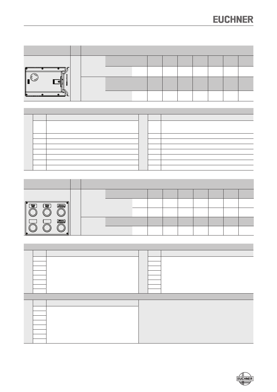
Data block for MGB evaluation module L0, L1 or L2
MGB module
Slot
Required memory in data range of the control system (IO controller)
(Refer to the data sheet of your device for the exact bit allocation)
Locking module
(configuration example)
-S7
For slot assignment, see data
sheet
Input range
(1 byte)
Switch
ÜK
SK
-
-
-
Z
R
T
Bit
I0.7
I0.6
I0.5
I0.4
I0.3
I0.2
I0.1
I0.0
Output range
(1 byte)
Display
-
-
-
-
-
-
-
Guard
locking
solenoid
Bit
O0.7
O0.6
O0.5
O0.4
O0.3
O0.2
O0.1
O0.0
Bit allocation
Input range
Bit
Description
Output range
Bit
Description
I0.0
T (door position)
O0.0
Guard locking solenoid – control voltage on
(function identical to bit
SO0.0 => but control from PROFINET
area)
I0.1
R (bolt position)
O0.1
n.c.
I0.2
Z (guard locking)
O0.2
n.c.
I0.3
n.c.
O0.3
n.c.
I0.4
n.c.
O0.4
n.c.
I0.5
n.c.
O0.5
n.c.
I0.6
SK (T AND R)
O0.6
n.c.
I0.7
ÜK (T AND R AND Z)
O0.7
n.c.
Data block for MGB control module
MGB module
Slot
Required memory in data range of the control system (IO controller)
(Refer to the data sheet of your device for the exact bit allocation)
Control module
(configuration example)
S12
S13
S14
S15
S11
S10
For slot assignment, see data
sheet
Input range
(2 bytes)
Switch
S17
S16
S15
S14
S13
S12
S11
S10
Bit
I0.7
I0.6
I0.5
I0.4
I0.3
I0.2
I0.1
I0.0
I1.7
I1.6
I1.5
I1.4
I1.3
I1.2
I1.1
I1.0
Output range
(1 byte)
Display
H17
H16
H15
H14
H13
H12
H11
H10
Bit
O0.7
O0.6
O0.5
O0.4
O0.3
O0.2
O0.1
O0.0
Bit allocation for 1st byte
Input range
Bit
Description
Output range
Bit
Description
I0.0
Depends on your configuration variant (refer to the data
sheet of your device for the exact bit allocation)
O0.0
Depends on your configuration variant (refer to the data
sheet of your device for the exact bit allocation)
I0.1
O0.1
I0.2
O0.2
I0.3
O0.3
I0.4
O0.4
I0.5
O0.5
I0.6
O0.6
I0.7
O0.7
Bit allocation for 2nd byte
Input range
Bit
Description
I1.0
Depends on your configuration variant (refer to the data
sheet of your device for the exact bit allocation)
I1.1
I1.2
I1.3
I1.4
I1.5
I1.6
I1.7
