Digital audio interface (dai), Codec interface, Ssi2 interface – Cirrus Logic EP7309 User Manual
Page 7
DS507F2
Copyright Cirrus Logic, Inc. 2011
(All Rights Reserved)
7
EP7309
High-Performance, Low-Power System on Chip
rates up to 115.2 kbps. An IrDA SIR protocol encoder/decoder
can be optionally switched into the RX/TX signals to/from
UART 1 to enable these signals to drive an infrared
communication interface directly.
Digital Audio Interface (DAI)
The EP7309 integrates an interface to enable a direct
connection to many low cost, low power, high quality audio
converters. In particular, the DAI can directly interface with
the Crystal
‚
CS43L41/42/43 low-power audio DACs and the
Crystal
‚
CS53L32 low-power ADC. Some of these devices
feature digital bass and treble boost, digital volume control and
compressor-limiter functions.
Note:
See
for information on pin
multiplexes.
CODEC Interface
The EP7309 includes an interface to telephony-type CODECs
for easy integration into voice-over-IP and other voice
communications systems. The CODEC interface is
multiplexed to the same pins as the DAI and SSI2.
Note:
See
for information on pin
multiplexes.
SSI2 Interface
An additional SPI/Microwire1-compatible interface is
available for both master and slave mode communications. The
SSI2 unit shares the same pins as the DAI and CODEC
interfaces through a multiplexer.
•
Synchronous clock speeds of up to 512 kHz
•
Separate 16 entry TX and RX half-word wide FIFOs
•
Half empty/full interrupts for FIFOs
•
Separate RX and TX frame sync signals for asymmetric
traffic
Note:
See
for information on pin
multiplexes.
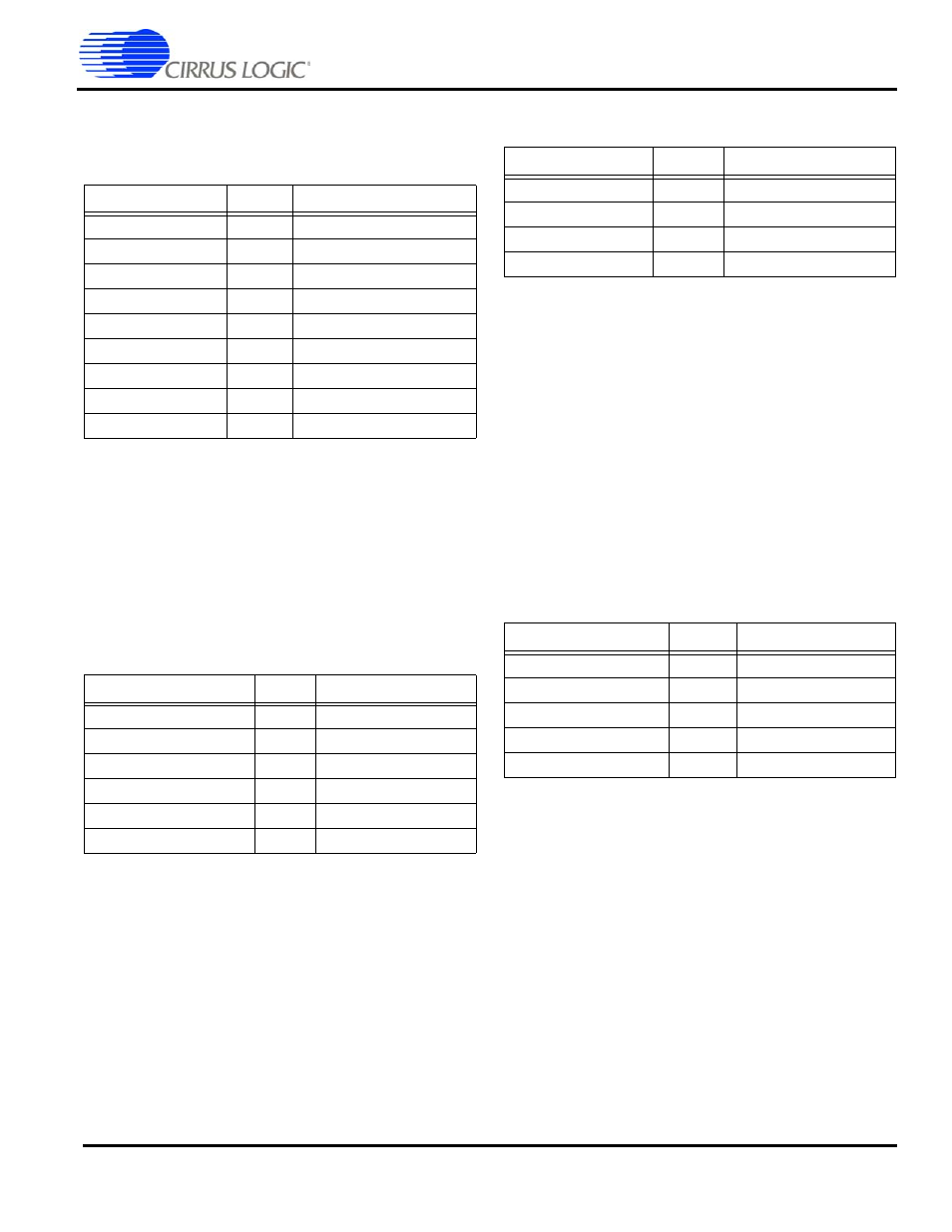
Pin Mnemonic
I/O
Pin Description
TXD[1]
O
UART 1 transmit
RXD[1]
I
UART 1 receive
CTS
I
UART 1 clear to send
DCD
I
UART 1 data carrier detect
DSR
I
UART 1 data set ready
TXD[2]
O
UART 2 transmit
RXD[2]
I
UART 2 receive
LEDDRV
O
Infrared LED drive output
PHDIN
I
Photo diode input
Table 3. Universal Asynchronous Receiver/Transmitters Pin
Assignments
Pin Mnemonic
I/O
Pin Description
SCLK
O
Serial bit clock
SDOUT
O
Serial data out
SDIN
I
Serial data in
LRCK
O
Sample clock
MCLKIN
I
Master clock input
MCLKOUT
O
Master clock output
Table 4. DAI Interface Pin Assignments
Pin Mnemonic
I/O
Pin Description
PCMCLK
O
Serial bit clock
PCMOUT
O
Serial data out
PCMIN
I
Serial data in
PCMSYNC
O
Frame sync
Table 5. CODEC Interface Pin Assignments
Pin Mnemonic
I/O
Pin Description
SSICLK
I/O
Serial bit clock
SSITXDA
O
Serial data out
SSIRXDA
I
Serial data in
SSITXFR
I/O
Transmit frame sync
SSIRXFR
I/O
Receive frame sync
Table 6. SSI2 Interface Pin Assignments