Ds507f2 – Cirrus Logic EP7309 User Manual
Page 33
DS507F2
Copyright Cirrus Logic, Inc. 2011
(All Rights Reserved)
33
EP7309
High-Performance, Low-Power System on Chip
P6
VSSIO
Pad ground
I/O ground
P7
VSSIO
Pad ground
I/O ground
P8
VDDIO
Pad power
Digital I/O power, 3.3V
P9
VSSIO
Pad ground
I/O ground
P10
VDDIO
Pad power
Digital I/O power, 3.3V
P11
VSSIO
Pad ground
I/O ground
P12
VSSIO
Pad ground
I/O ground
P13
VDDIO
Pad power
Digital I/O power
P14
VSSIO
Pad ground
I/O ground
P15
D[24]
I/O
Data I/O
P16
VDDIO
Pad power
Digital I/O power, 3.3V
R1
RTCIN
I/O
Real time clock oscillator input
R2
VDDIO
Pad power
Digital I/O power, 3.3V
R3
PD[4]
I/O
GPIO port D
R4
PD[1]
I/O
GPIO port D
R5
SSITXDA
O
DAI/CODEC/SSI2 serial data output
R6
nADCCS
O
SSI1 ADC chip select
R7
VDDIO
Pad power
Digital I/O power, 3.3V
R8
ADCOUT
O
SSI1 ADC serial data output
R9
COL[7]
O
Keyboard scanner column drive
R10
COL[3]
O
Keyboard scanner column drive
R11
COL[1]
O
Keyboard scanner column drive
R12
D[30]
I/O
Data I/O
R13
A[27]
O
System byte address
R14
A[25]
O
System byte address
R15
VDDIO
Pad power
Digital I/O power, 3.3V
R16
A[24]
O
System byte address
T1
VDDRTC
RTC power
Real time clock power, 2.5V
T2
PD[7]
I/O
GPIO port D
T3
PD[6]
I/O
GPIO port D
T4
PD[3]
I/O
GPIO port D
T5
SSICLK
I/O
DAI/CODEC/SSI2 serial clock
T6
SSIRXFR
–
DAI/CODEC/SSI2 frame sync
T7
VDDCORE
Core power Core power, 2.5V
T8
DRIVE[0]
I/O
PWM drive output
T9
FB[1]
I
PWM feedback input
T10
COL[5]
O
Keyboard scanner column drive
T11
VDDIO
Pad power
Digital I/O power, 3.3V
T12
BUZ
O
Buzzer drive output
T13
D[28]
I/O
Data I/O
T14
A[26]
O
System byte address
T15
D[25]
I/O
Data I/O
T16
VSSIO
Pad ground
I/O ground
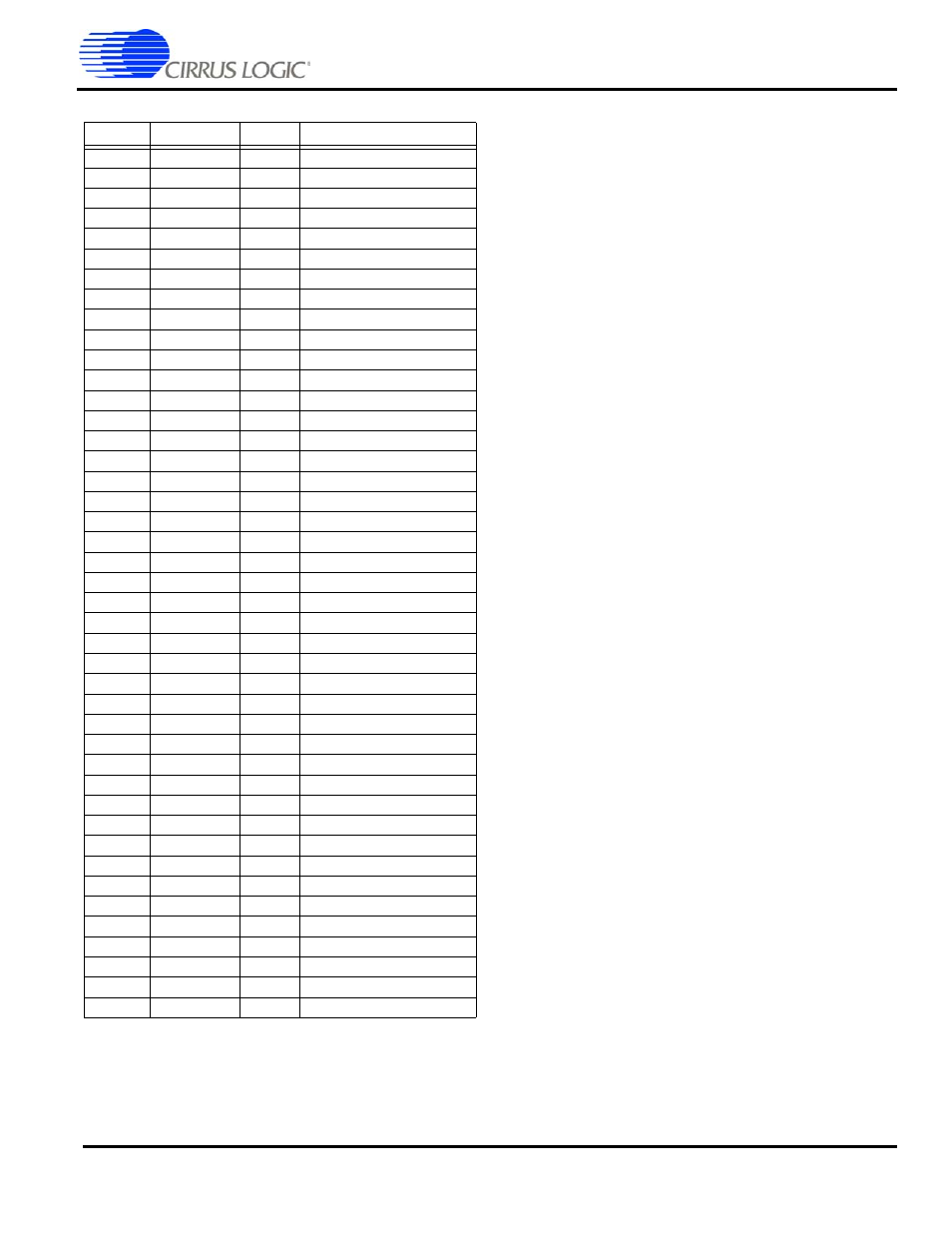
Table 20. 256-Ball PBGA Ball Listing (Continued)
Ball Location
Name
Type
Description